For any type of power conversion device, the automotive and heavy equipment vehicle environment requirements are very demanding. Wide operating voltage ranges combined with large transients and temperature variations make designing reliable electronic systems difficult. A further complicating factor in design considerations is the increasing number of voltage rails within an electronic system. For example, a typical navigation system might have six or more voltage rails, including 8.5V, 5V, 3.3V, 2.5V, 1.8V, and 1.5V. At the same time, as the number of components increases, the available space continues to shrink, making high-efficiency conversion critical due to space constraints and high temperature conditions.
As a result, good switching DC/DC regulators for cars and trucks must be specified to operate over a wide input voltage range. For a 12V system, the 60V rating provides a good margin, and such systems are typically clamped in the 36V to 40V range. In addition, the dual battery applications seen in trucks and heavy equipment require a higher operating voltage due to the nominal battery voltage of 24V. Most of these applications are clamped to 58V, so a 60V rating is usually sufficient. Overvoltage clamps built into cars and trucks are needed to limit the maximum transient voltage caused by the inductive retrace voltage of the engine starter, which, if not clamped, can cause much larger transient voltages.
There are many car and truck systems that require continuous power supply even when the vehicle's electric motor is not running, such as remote door opening systems and alarm systems. This type of "always on" system necessitates a DC/DC converter with low quiescent current to maximize battery run time while in sleep mode. In this type of environment, the regulator operates in a normal continuous switching mode until the output current drops below a predetermined threshold of approximately 30 mA to 50 mA. Below this threshold, the switching regulator must go into Burst Mode? operation to reduce the quiescent current to tens of microamps, reducing the power drawn from the battery to extend battery run time.
Faced with a shortage of 60V input DC/DC converters, some designers turned to a transformer-based topology or an external high-side driver to operate at up to 60V. Other designers have adopted an intermediate bus converter that requires an additional power stage. Both types of replacement solutions increase the complexity of the design and, in most cases, reduce overall efficiency. However, Linear Technology has introduced the LTC3890, the latest addition to a growing family of 60V input step-down switching regulator controllers that address many of the key issues in these automotive and truck applications. Figure 1 shows the working principle of the LTC3890 in an application that converts 9V to 60V inputs to 3.5V/5A and 8.5V/3A outputs.
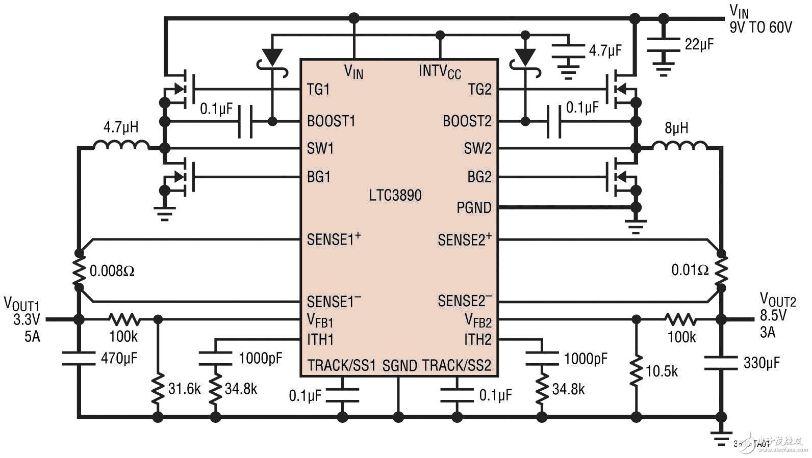
Figure 1: LTC3890 Schematic Conversion of 9V to 60V Inputs to 8.5V/3A and 3.3V/5A Outputs
The LTC3890/-1 is a high voltage, dual output synchronous step-down DC/DC controller that draws only 50uA from one output while only 60uA is drawn when both outputs are enabled. When both outputs are turned off, the LTC3890/-1 draws only 14uA. The device's 4V to 60V input voltage range is designed to protect against high voltage transients and to maintain continuous operation in heavy equipment vehicles and trucks that are cold-run and cover multiple input power and battery chemistries. Each output can be set to 0.8V to 24V at output currents up to 20A with up to 98% efficiency, making the device ideal for 12V or 24V automotive, truck, heavy equipment and industrial control applications.
The LTC3890/-1 operates from an optional fixed frequency range of 50kHz to 900kHz and can be synchronized to an external clock from 75kHz to 850kHz with a phase-locked loop (PLL). At light loads, the user can select continuous operation, pulse skipping, and low ripple burst mode operation. The two-phase operation of the LTC3890 reduces input filtering and capacitance requirements. Its current mode architecture provides very easy loop compensation, fast transient response and excellent voltage regulation. Output current sensing is achieved by measuring the voltage drop across the output inductor (DCR) for maximum efficiency or for output current sensing using an optional sense resistor. In the event of an overload, current foldback limits the amount of heat generated by the MOSFET. These features, combined with a minimum turn-on time of only 95ns, make the controller ideal for high step-down ratio applications.
Available in two versions, the LTC3890 is a full-featured device that includes clock output, clock phase modulation, two separate power good outputs, and adjustable current limit. The LTC3890-1 does not have these additional features and is available in a 28-pin SSOP package. The LTC3890 is available in a 32-lead 5mm x 5mm QFN package.
Burst mode operation, pulse skipping or forced continuous mode
At low load currents, the LTC3890/-1 can enter high efficiency burst mode operation, constant frequency pulse skipping or forced continuous conduction mode at startup. When configured to operate in burst mode and in a light load condition, the converter will generate several pulses in a burst to maintain the charging voltage on the output capacitor. The converter then turns off and enters sleep mode, where most of the internal circuitry of the converter is turned off. At this time, the load current is supplied by the output capacitor. When the voltage across the output capacitor drops to a set value, the converter resumes the burst mode operation, thereby providing a larger current to supplement the charging voltage. Turning off most of the internal circuitry greatly reduces the quiescent current, which helps to extend battery run time when the system is not running in a "always on" system. Figure 2 shows a conceptual timing diagram for the above work process.
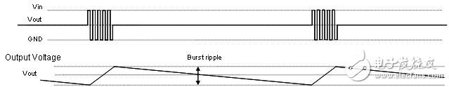
Figure 2: Voltage Timing Diagram for LTC3890 Burst Mode Operation
Switch Node Voltage: Switch Node Voltage
Output Voltage: Output voltage
Burst triple: burst ripple
Burst mode output ripple is unaffected by the load, so only the length of the sleep interval will change. In sleep mode, most of the internal circuitry is turned off, except for critical circuits that require fast response, further reducing quiescent current. When the output voltage drops low enough, the sleep signal goes low and the controller turns on the external MOSFET at the top to resume normal burst mode operation. In addition, there are some examples of users operating in forced continuous or constant frequency pulse skip mode at light load currents. Both modes are very easy to configure, but have large quiescent current and small peak-to-peak output ripple.
In addition, the inductor current is not allowed to reverse when the controller is started to operate in burst mode. The reverse current comparator IR turns off the bottom external MOSFET before the inductor current will reach zero, preventing the current from becoming negative. Therefore, when configured for burst mode operation, the controller also operates in discontinuous mode.
In addition, the inductor current is allowed to reverse during light load or large transient conditions when forced continuous operation or clocking by an external clock source. The advantage of continuous operation is that the output voltage ripple is small, but produces a large quiescent current.
Overcurrent protection
Fast and accurate overcurrent limiting protection is necessary in high voltage power supplies. Because the output is short-circuited, high voltage appears across the inductor, so either use a sense resistor in series with the output or use a voltage drop across the output inductor to sense the output current. Either way, the output current is continuously monitored and provides the highest level of protection. Some alternative designs may use the RDS(ON) of the top or bottom MOSFET to sense the output current. However, this causes the controller to be unaware of the output current for a period of time during the switching cycle, which may cause the converter to malfunction.
Powerful gate drive
Switching losses are proportional to the square of the input voltage, and when the gate drivers are not powerful enough, such losses can have a significant impact in high input voltage applications. The LTC3890/-1 features a powerful 1.1? internal N-channel MOSFET gate driver that minimizes conversion time and switching losses to maximize efficiency. In addition, the device can drive multiple parallel MOSFETs in higher current applications.
effectiveness
The efficiency curve of the LTC3890 in Figure 3 is a typical efficiency curve for the schematic of Figure 1 with a 12V input voltage. As shown, the 8.5V output produces very high (up to 98%) efficiency. The efficiency is also over 90% at 3.3V. In addition, this design works in burst mode, so the efficiency is still over 75% for each output with 1mA load.
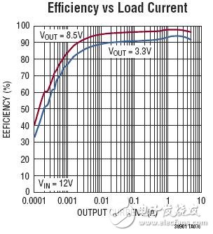
Figure 3: Efficiency curve of the LTC3890 at 12V input, 8.5V and 3.3V output
Efficiency vs Load Current: Efficiency vs. load current
OUTPUT CURRENT: Output current
Fast transient response
The LTC3890 implements voltage feedback using a fast amplifier operating at 25MHz bandwidth. The amplifier has a large bandwidth and high switching frequency and low value inductors, thus allowing very high gain crossover frequencies. This allows the compensation network to be optimized for very fast load transient response. Figure 4 illustrates the transient response of a 3.3V output, 4A step load, which deviates from the nominal value by less than 100mV.
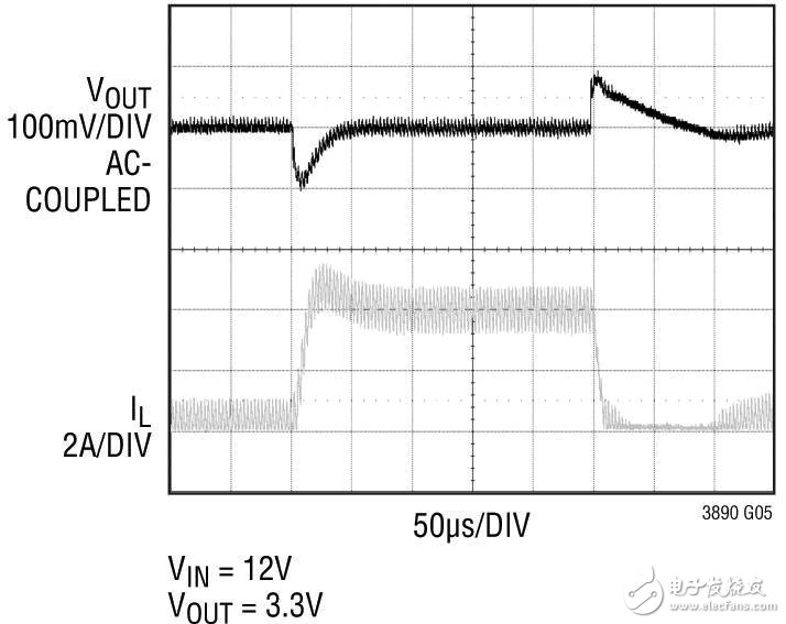
Figure 4: Transient response curve of the LTC3890 at 4A step load
AC-COUPLED: AC coupling
50us/DIV: 50us per cell
in conclusion
The LTC3890 offers a variety of features that make it ideal for high input voltage power supplies. The device offers new levels of performance in terms of the need to operate safely and efficiently in demanding high voltage transient environments. The device's features include 60V input capability, making it ideal for automotive dual battery, truck and heavy equipment applications. Its low quiescent current saves battery power during sleep mode, which extends battery run time, which is very useful in bus systems that are “always onâ€.
In addition, the LTC3890 is easy to apply to a variety of output voltages, including output voltages up to 24V. In addition, its shortest turn-on time is short, which allows the LTC3890 to be used in high step-down ratio applications. The device reduces the input voltage directly from 60V, or external protection, without the need for a clumsy transformer, which helps to create a cost-effective, compact and reliable solution.
T Copper Tube Terminals,Non-Insulated Pin-Shaped Naked Terminal,Copper Cable Lugs Terminals,Insulated Fork Cable Spade Terminal
Taixing Longyi Terminals Co.,Ltd. , https://www.longyiterminals.com