Digital down-conversion is an important part of the wireless communication link layer. The down-conversion of wideband signals and narrow-band signals differs due to different signal bandwidths, making it difficult to implement systems with both wideband and narrowband signals using FPGA-based systems. In this paper, the dedicated digital down-conversion frequency chip GC5016 is used to realize the conversion of wideband and narrowband signals simultaneously. The reception and storage of wide/narrowband data is realized by FPGA. After storage, the data is processed by high-performance DSP chip C6455. The software and hardware design method of the system is introduced in detail.
introductionWith the development of electronic technology and signal processing technology, the application of broadband data is increasing, and narrow-band data communication is still widespread. At the same time, processing broadband and narrowband data is a problem encountered in wireless communication. In digital receiver systems, the requirements for wideband and narrowband data are not fixed in advance, but after signal analysis and identification, the transmission of broadband or narrowband signals is performed adaptively or by the user to issue commands on site. In this application background, FPGA-based digital down conversion faces field programming problems. The general FPGA solution is to store various bandwidth parameters in its FLASH chip, and call operating parameters under different bandwidths according to commands at any time, but The required storage space is large, and the resources of the FPGA are also large. The system designed based on this method requires a large-capacity FPGA chip, and the system consumes a large amount of power and has a high price.
To this end, this paper proposes a wide/narrowband data down-conversion solution based on the dedicated digital down-conversion chip GC5016. The small-scale FPGA is used to read and store the GC5016 output data. The high-performance DSP chip C6455 is used to achieve the down-conversion. Analysis and demodulation of data.
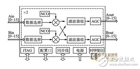
1 GC5016 and its structureThe GC5016 is a wideband 4-channel programmable digital up-and-down converter from TI that offers an input rate of 160 Msps and can handle up to 320 Msps of input rate in dual-channel joints to meet the speed requirements of most A/D devices today. The four identical channels can be independently configured for upconversion, downconversion or a combination of two upconversions and two downconversions. This article mainly introduces its down conversion function. The internal structure of the GC5016 is shown in Figure 1. The figure shows the structure of the GC5016 in the receiving mode. There are 4 channels inside. The figure shows the structure of the two channels A and B. The channels C and D have the same consistency with the two channels. structure.

Figure 1 Internal structure of GC5016
The input data enters the mixer through the data selection unit, and the data selection format has three formats: fixed point 16 bits, floating point 16 bits, and AB dual synthesized data. The digital mixer will mix the signals according to the software configuration. In order to facilitate the subsequent filtering, the data is generally converted to zero-frequency centered baseband data. The baseband data can be separately synthesized through two filters, or each filter can be separately filtered. The filter bank includes a CIC filter and a programmable filter: the CIC filter can realize integer extraction from 1 to 256, which reduces the data rate; the programmable filter generally uses an FIR filter to further extract and shape the signal, where the extraction can be performed. For 1~16, it can be seen that GC5016 can achieve a maximum decimation of 4 096 (16 256). The FIR filtered data passes through the AGC power detection and control module, and the data is finally outputted after being formatted.
The configuration port in the figure is a parallel data interface. The register of GC5016 must be configured through this interface. The register of the chip can also be read through the configuration port to check whether the chip works normally and the initialization is correct. The GC5016 has a synchronous input and synchronous output. Port, can be used for synchronization of multiple GC5016, can also be used for synchronization of several channels in a single chip; JTAG port is used for chip testing, users generally do not need to connect; power supply and clock reset interface is the basic configuration of chip normal operation .
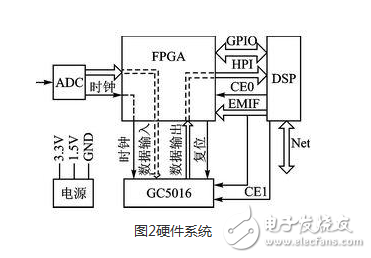
2 hardware system designThe hardware system is mainly composed of ADC, GC5016, FPGA and DSP, as shown in Figure 2.

Figure 2 hardware system
The analog-to-digital converter chip ADC uses the Analog Devices 16-bit chip AD9467, which has a sampling frequency of up to 200 MHz, 75 SNR and 90 dB SFDR, making it a high-performance ADC with high performance. The external interface is differential LVDS data and clock bus. The differential output cannot be directly connected to the GC5016. The FPGA needs to convert the differential signal into a single-ended signal. The FPGA reads and converts the differential data with the differential clock output from the ADC as the reference clock, and the processed single-ended signal data is still output to the GC5016 under the clock reference. Since the differential port of the FPGA is corresponding, the differential data line and the differential clock line connected to the ADC should be careful not to be connected randomly. Try to arrange them in the same bank of the FPGA. Otherwise, the transmission path may be inconsistent and easy to read and write under high-speed data. Phase distortion is generated, making input and transmission data errors.
The data between the DSP and the FPGA is written to the DSP through the HPI interface, which saves the data read and write time of the DSP. There is also an EMIF interface between the DSP and the FPGA for DSP control of the FPGA. The control state between the DSP and the FPGA is transmitted by the GPIO bus. At the same time, the DSP also connects an EMIF interface to the GC5016 for DSP control and status reading of the GC5016.
3 software design 3.1 GC5016 control register settingsFork Type Connecting Terminals
Fork Type Connecting Terminals,Terminals,Connecting Terminals
Taixing Longyi Terminals Co.,Ltd. , https://www.longyicopperlugs.com