With the development of mobile communication technology, research on radio frequency (RF) circuits has attracted extensive attention. Implementing a voltage-controlled oscillator (VCO) in a standard CMOS process is key to implementing an RF CMOS integrated transceiver. In the past, most of the VCO circuits used reverse-biased varactors as voltage-controlled devices. However, when the circuit was implemented by the actual process, it was found that the quality factor of the varactors was usually small, which would affect the performance of the circuit. Therefore, people tried to replace the general varactor diode with other devices that can be implemented in CMOS technology, and MOS varactors came into being.
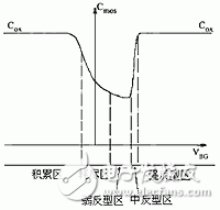
MOS varactor Shorting the drain, source and substrate of the MOS transistor can be a simple MOS capacitor whose capacitance varies with the voltage VBG between the gate and the substrate. In the PMOS capacitor, the inversion carrier channel is established when VBG is greater than the absolute value of the threshold voltage. When VBG is much larger than the absolute value of the threshold voltage, the PMOS capacitor operates in a strong inversion region. On the other hand, when the gate voltage VG is larger than the substrate voltage VB, the PMOS capacitor operates in the accumulation region, at which time the interface voltage between the gate oxide layer and the semiconductor is positive and the electrons can move freely. Thus, the PMOS capacitance value Cmos in the inversion region and the accumulation region is equal to Cox (oxide layer capacitance).
There are three working areas between the strong inversion zone and the accumulation zone: the middle inversion zone, the weak inversion zone and the depletion zone. There are only a few mobile carriers in these working areas, which reduces the Cmos capacitance (less than Cox). At this time, Cmos can be regarded as a series connection of Cox and Cb and Ci parallel capacitors. Cb represents the closed loop of the depletion region capacitance, and Ci is related to the amount of change in the number of holes at the gate oxide interface. If Cb(Ci) dominates, the PMOS device operates in the depleted (medium-inverse) region; if both capacitors are not dominant, the PMOS device operates in the weak inversion region. The curve of Cmos capacitance value with VBG is shown in Figure 1.
Modulation characteristic curve of pmos capacitor with b=d=s
The channel parasitic resistance of a PMOS operating in a strong inversion region can be derived from:
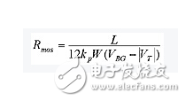
Where W, L and kp are the width, length and gain factor of the PMOS transistor, respectively. It is worth noting that as VBG approaches the absolute value of the threshold voltage, Rmos gradually increases, and Rmos is infinite when VBG is equal to the absolute value of the threshold voltage. This formula is based on the simplest PMOS model. In fact, as the hole concentration decreases steadily, Rmos will remain finite throughout the mid-inversion region.
Inverse and accumulation MOS varactor From the above analysis, we know that the tuning characteristics of ordinary MOS varactors are non-monotonic. There are two ways to obtain monotonic tuning characteristics.
One method is to ensure that the transistor does not enter the accumulation region if the VG varies widely, which can be done by disconnecting the substrate from the gate source junction and shorting the highest DC voltage in the circuit (eg, supply voltage Vdd). .
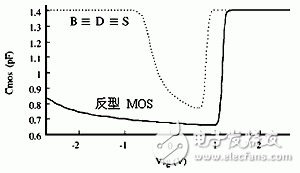
It is obvious that the tuning range of the inversion MOS capacitor is wider than that of the ordinary MOS capacitor. The former only works in the strong, medium and weak inversion regions, and never enters the accumulation region.
A better approach is to apply MOS devices that only operate in the depletion and accumulation regions, which results in a larger tuning range and lower parasitic resistance, which means a higher quality factor because it is depleted. The electrons in the region and the accumulation region are multi-carriers, which are about three times higher than the mobility of holes. To obtain an accumulation type MOS capacitor, it is necessary to ensure that the strong inversion region, the middle inversion region, and the weak inversion region are prohibited, which requires suppressing the channel of any hole injecting MOS. The method is to remove the p-doping of the drain-source junction in the MOS device, and at the same time make the n-doped substrate contact at the position of the original drain-source junction, as shown in FIG.
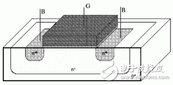
Thus, the parasitic resistance of the n-well is reduced to the tuning curve of the most accumulated MOS capacitor and the common MOS capacitor as shown in FIG.
Modulation characteristic curve of accumulated MOS capacitorFig. 4 Modulation characteristic curve of the accumulation type MOS capacitor It can be seen that the accumulation type MOS capacitance is excellent in monotonicity. It is worth noting that no additional process flow was introduced in the process of designing the accumulated MOS capacitor.
Design and simulation resultsVco circuit diagram
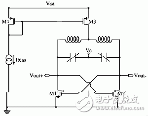
The structure of the VCO circuit used by the author is shown in Figure 5. This is a standard symmetrical CMOS structure. The two varactors are symmetrically connected, which reduces the influence of the potential change on the varactor capacitance when both ends oscillate, and improves the spectral purity. In order to ensure good matching, the inductors should use the same dual inductance symmetrical connection. In addition, since the LC tank circuit consists of two very large on-chip integrated inductors and two equally large cumulative MOS varactors, the higher loss results in a lower quality factor, which requires a larger The negative transconductance is used to maintain the oscillation continuously; and the absolute value of the equivalent negative transconductance must be larger than the transconductance value required to maintain the constant amplitude oscillation to ensure the oscillation, so the two pairs of coupling transistors need to set a larger aspect ratio. However, the large aspect ratio causes a large parasitic effect, which causes phase noise and tuning range to be affected. Finally, two NMOS transistors are used at the bottom to form a negative resistance to compensate for the VCO loss. According to the small-signal model analysis, the absolute value of the equivalent negative resistance RG can be estimated by ignoring various parasitic and high-order effects (the two active devices are transposed to gM1, gM2, respectively):

The top PMOS transistor provides a bias current and the required supply voltage is low. The entire design is based on TSMC's 0.35μm silicon-silicon RF process model PDK, which has three layers of metal. Among them, the inductor is a flat spiral octagon, which is made of a top metal. If the inductance value is 0.6nH, then the total capacitance can be determined to constitute the parasitic capacitance of the capacitor component in the LC oscillator circuit with inductance (small), the drain-substrate capacitance of the NMOS transistor, and the gate. - Leakage capacitance, gate-source capacitance and most important accumulation MOS capacitors. In the case of guaranteed start-up, in order to obtain a larger tuning range, the proportion of the last item must be as large as possible.
Vco tuning curve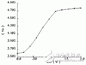
The final power supply voltage is 1.5V and the power consumption is about 10mW. The simulation is performed by SpectreRF under the Cadence platform, and the obtained tuning curve is shown in Fig. 6. When the control voltage changes from 0 to 2V, the oscillation frequency varies from 3.59 to 4.77 GHz, the center frequency is 4.18 GHz, and the tuning range is about 28%. The phase noise curve at the center frequency is shown in Fig. 7. The control voltage at this time is 0.75V, and the phase noise corresponding to the offset of 600kHz is -128dB/Hz.
Vco phase noise curve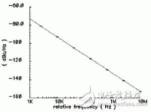
When the control voltage is changed from 0.75V to 2V, the oscillation frequency becomes 4.77GHz, and the phase noise becomes -135dB/Hz, which is reduced by 7dB. This is caused by two reasons. First, because the total capacitance of the LC tank is reduced, the oscillation frequency is increased, which reduces the negative transconductance required to maintain the oscillation, but because of the two NMOS transistors. The negative transconductance is almost constant, so the amplitude of the stable oscillation is increased, and the phase noise is reduced. On the other hand, the channel parasitic resistance of the accumulated MOS capacitor is reduced as the voltage increases, thereby reducing the voltage. Loss, reducing phase noise.
Compared with the VCO with inverted MOS varactor design, due to the higher mobility of electrons, the channel parasitic resistance of the accumulation MOS capacitor is lower than that of the inverse MOS capacitor, which means that the accumulation MOS capacitor has higher The quality factor has led to an increase in the overall performance of the VCO, especially with reduced phase noise. The comparison results are shown in Table 1. Considering the process and power consumption factors, the use of accumulated MOS capacitors has a greater advantage.

Based on the 0.35μm process, considering a low voltage and low power consumption, a VCO operating at 4.2 GHz is designed, and the accumulated MOS capacitor and the inversion MOS capacitor are used for tuning in the circuit. The simulation results show that the two VCO tuning ranges are almost the same as the center frequency. The accumulated MOS-tuned VCO exhibits better phase noise performance when the power consumption is about 10mW.
Lithium Battery 2Cr11108,Marine Lithium Battery,Lithium Battery Smoke Alarms,Manganese Dioxide Lithium Battery
Jiangmen Hongli Energy Co.ltd , https://www.honglienergy.com