This article introduces the ARM core S3C2440 as the processor, 24-bit ADS1256 chip with analog switch for A / D conversion and signal input channel selection, using its characteristics, working principle to design with high precision, multi-channel, real-time operation Strong seismic data acquisition system circuit. The data is input through the bridge low-pass filter, which effectively suppresses the long-wire common mode signal and greatly improves the anti-electromagnetic interference capability of the entire circuit, thereby realizing high precision, high quality, low power consumption and portable of the seismic data acquisition system. Features.
System overall structure block diagramThe overall structure of the circuit is shown in Figure 1. The ARM9 series S2C2440 microprocessor produced by Samsung is used as the core control chip. The weak and complex seismic signals output by the geophone are first amplified, followed and filtered by the analog signal conditioning circuit. After that, the channel is selected by controlling the analog switch, and then the ADS1256 is used for analog-to-digital conversion. The collected data is sent to the mass storage through the SPI bus for later reference and analysis.

The analog signal conditioning circuit mainly includes filtering and amplification of seismic weak signals. The seismic signal is first passed through an input circuit formed by bridge low-pass filtering and then through a preamplifier circuit.
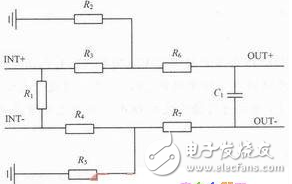
The input circuit mainly functions as an RC impedance matching network, suppressing the common mode signal in the long wire transmission, blocking the high frequency signal, improving the anti-interference ability, and suppressing the interference wave received from the effective wave recording. The principle is shown in Figure 2.

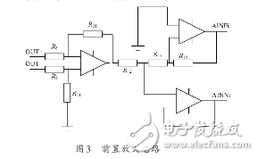
The preamplifier circuit is mainly composed of two stages, and the two stages are connected by direct coupling. The first stage amplifies the double-ended input seismic signal, then single-stage output, and then passes through the second-stage differential linear amplifier to convert the output mode to A. The /D conversion provides a double-ended input differential signal, which further eliminates the common-mode signal of the input circuit. The circuit principle is shown in Figure 3. In order to ensure that the input terminal is in equilibrium, the resistance values ​​of the two input terminals to ground should be equal. In order to reduce the common mode voltage amplification, R7=R8 and R9=R10 are generally used.

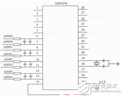
Using the ARM processor to control the ADS1256 as an analog-to-digital conversion circuit, the ADS1256 can only operate in SPI communication mode. The design uses the general-purpose I/O port of the ARM processor to control the ADS1256 on-chip registers. It can also read/write these registers through the serial port, and select whether to start conversion by controlling the CS signal of the ADS1256. The level of the DRDY pin is read to indicate whether the conversion has been completed. A low level indicates that the data conversion is complete, and a high level indicates that the data conversion is not completed. Read the latest conversion data from the DOUT pin, control the internal analog switch register to configure the four-channel differential input, and use AINO~AIN7 as the input terminal. AINCOM is not used. Generally, it can be grounded. PSEN3~PSEN0 are the positive input terminals of the differential signal. Bits, NSEL3~NSEL0, are the negative input selection bits of the differential signal. Use the ADCON register to configure the output clock, sensor detection selection, and program-controlled amplification. CLK1 and CLK0 are the output clock selection bits. Where: 00 means the output clock is off; 01 means the output fCLKIN; 10 means the output fCLKIN/2; 11 means the output fCLKIN/4, the main clock is provided by the external crystal, the crystal is 7.68 MHz, PGA2 ~ PGA0 is the amplification of the programmable gain amplifier Bits: 000=1,001=2,010=4,011=8,100=16,101=32,110=64,111=128, the register can be configured according to the strength of the signal. DIR7~DIR0 are data rate selection bits, and 11110000=30 kS/s is the default value. In this way, each register can be controlled by software programming to flexibly configure the required clock output, sensor detection selection, program-controlled amplification factor, data conversion rate, and the like. Its control circuit connection is shown in Figure 4.

When the PCB board is wired, the crystal oscillator must be close to the ADS1256. To ensure the start-up and obtain a stable frequency, a ceramic capacitor of less than 0.1μF must be connected externally. The system takes 18 pF.
Peripheral interface circuitThe main interface circuit includes a touch display circuit, a storage circuit and a host computer communication circuit, etc., which is basically similar to the interface circuit on the development board, and only a simple text description is made here. The circuit mainly uses extended FLASH and SDRAM for system startup and running program loading. FLASH is used to store the user's program code, and SDRAM is used to store the program running data and a small amount of data. The display part adopts a liquid crystal display device of a flat type structure, and has excellent characteristics of displaying large amount of information, low voltage, low power consumption, long life, no radiation, no pollution, and occupies an important position in the display field. Generally, the indirect access method is used to realize the circuit connection between the controller chip and the liquid crystal display module. The data of the liquid crystal display module usually needs to be input in parallel. Here, it is necessary to apply the serial conversion and the device to serial/parallel conversion to provide parallel input for the liquid crystal display. Control signals such as read, write, chip select, and reset of the module are controlled by the general-purpose I/O pins of the S3C2440. The high-speed USB bus transmission technology is selected to communicate with the host computer. This implementation must be done together with the S3C2440 and the dedicated USB communication driver chip and peripheral circuits. In order to facilitate the hardware debugging of the USB interface, an RS 232 interface must be added.
A manual pulse generator (MPG) is a device normally associated with computer numerically controlled machinery or other devices involved in positioning. It usually consists of a rotating knob that generates electrical pulses that are sent to an equipment controller. The controller will then move the piece of equipment a predetermined distance for each pulse.
The CNC handheld controller MPG Pendant with x1, x10, x100 selectable. It is equipped with our popular machined MPG unit, 4,5,6 axis and scale selector, emergency stop and reset button.
Manual Pulse Generator,Handwheel MPG CNC,Electric Pulse Generator,Signal Pulse Generator
Jilin Lander Intelligent Technology Co., Ltd , https://www.jilinlandermotor.com