The Fution series FPGA is the world's first ADC-based analog-digital hybrid FPGA. It adds the analog circuit part to the digital FPGA, which solves many problems caused by the separation of traditional analog circuits and FPGAs. The difficulty in making PCB boards reduces the size of the product. The programmability of the FPGA makes the system easy to upgrade. At the same time, the introduction of analog circuits in the digital system simplifies the system circuit design.
1 Fution FPGA Introduction The main features of Fution FPGA are mainly reflected in:
(1) Single chip: no need to configure the chip;
(2) High security: The transistor is protected by 7 layers of metal, with AES and Flash Lock encryption technology;
(3) High reliability: It has immunity to high-energy particle bombardment and has strong firmware error immune function;
(4) Power on: the power-on time is very short, generally only a few tens of microseconds;
(5) Low power consumption: Whether it is dynamic power or static power is lower than the competition, IGLOO can be as low as 5?
(6) Low system cost: no need to configure the chip, small power supply chip, no need for encryption chip, PCB area is smaller.
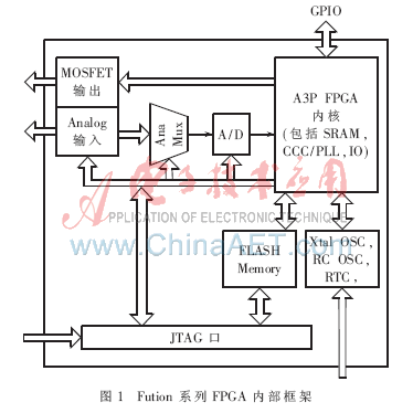
The internal framework of the Fusion series FPGA is shown in Figure 1.
This article refers to the address: http://
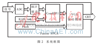
2 on-chip system implementation principle The on-chip system block diagram is shown in Figure 2. After the ECG signal collected by the ECG signal acquisition sensor is connected to the 12-bit ADC, the ADC converts the ECG analog signal into a digital signal and is latched by the BUF, and then sent to the Core8051 for acquisition and processing. The algorithm in Core8051 converts the data from the ADC into data that can be displayed by VGA, and then sends it to the VGA driver module.
2.1 ADC Module Design The Fution FPGA contains an AD converter with flexible sampling and conversion time, which provides a flexible AD conversion solution. As a successive approximation ADC, this converter has a sampling rate of up to 600 Ks/s, a 2.56 V reference source inside the device, and ±6 LSB of error in 12-bit mode with auto-calibration.
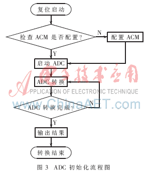
The ADC is configured by the internal logic unit of the FPGA: the ADC precision is set to 12 bits, the reference voltage is supplied with an on-chip voltage source with an amplitude of 2.56 V, and the ADC inside the FPGA has a Prescaler, so The flexibility to set the range of the sampling voltage further ensures the accuracy of the AD conversion. The ADC initialization process is as follows:
(1) Wait for the ADCRESET pin release to be invalid;
(2) After the ADCRESET pin is released, the ADC is powered on and self-calibrated;
(3) After power-on calibration (CALIBRATE=1), configure ACM;
(4) After the configuration is completed, the ADC is operated by ADC_START.
The FPGA internal logic unit performs ADC configuration and initialization to control ADC sampling. The specific process is shown in Figure 3.
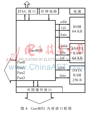
2.2 Control core Core8051 module design FPGA can embed high-speed Core 8051 processor core, it is the core of the whole system, responsible for orderly calling the rest of the functional modules, and at the same time has data processing tasks, responsible for the data from the ADC Convert to data that VGA can display. The Core8051's hardware configuration is very flexible, clock speed can reach 33 MHz, ROM size can be flexibly set according to needs, the design configuration is 64 KB. The on-chip DATA RAM only needs 256 B to complete the function of driving VGA, and can also expand the external 64 KB RAM to complete more powerful software functions. The on-chip DATA RAM of the microcontroller is set to 256 B, and the external 64 KB SRAM is extended by the system bus. The system block diagram is shown in Figure 4.
2.3 Color display driver module The development of mature TFT_LCD display driver is mostly based on ARM [2-3], DSP [4] platform. However, the processor used in this system is Coer8051, so there is no way to transplant the original driver module. Because the image data is relatively large, the processor computing power is relatively high. Therefore, combined with the characteristics of Core8051 and FPGA, an algorithm is redesigned to reduce the amount of data to be processed, thus completing the ECG image information within the capabilities of the Core8051. Display.
In order to display a complete image, one frame of image data prepared in advance is sequentially input to the data port in accordance with the clock sequence of the liquid crystal scanning, thereby completing display of one frame of image. Since the image to be displayed only has an electrocardiographic signal that changes dynamically, while the others are relatively stationary, that is, the data information does not change every scan, and the entire image is divided into dynamic (electrocardiogram). And static (background, scale) two parts. Dynamically generated by the Core8051 and input to the TFT_LCD at a specific time; static image information is stored in advance in the memory in the FPGA, and is input to the LCD in a specific order every scan. In this way, the Core 805 only needs to process the information of the ECG signal, thereby greatly reducing the processing amount of the image data and completing the display of the image. The module is designed to automate the real-time color interface that is difficult for low-end processors to implement, meaning that the 256-color interface can be displayed using only the Core8051 with 256 B RAM.
According to the above assumption, the liquid crystal panel can be divided into a dynamic portion and a static portion as shown in FIG.
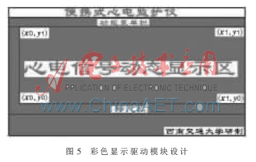
In Fig. 5, in addition to the "electrocardiographic signal dynamic display area", a dynamic electrocardiogram image is displayed, and other portions including the background image information in the "dynamic display area" are all stored in advance in the flash memory inside the FPGA.
The dynamic display area can be marked with two sets of data, set to: x0, y0, x1, y1, then the coordinates of each fixed point of the dynamic display area can be expressed as (x0, y0) (x0, y1) (x1, y0) ) (x1, y1). As shown in Fig. 5, the abscissa indicates the time t/s, the ordinate indicates the magnitude U/v of the electrocardiographic signal, and (x0, y0) is the (0, 0) coordinate point. Based on the Core8051, the coding algorithm is designed to encode the collected ECG signals, then convert the ECG signals into the coordinate signals of the display screen, and then calculate the ECG image data according to the coordinate signals, and under the control of the scan clock. The data is sequentially input to the LCD in order, so that the dynamic ECG image can be displayed.
The design of the ECG dynamic display area uses three methods, namely:
(1) Shift register method. A 240-bit shift register is built into the FPGA as a buffer for the ECG image. The Core8051 collects the data in real time and sends it to the shift register. At the same time, the CRT driver module continuously scans the shift register according to its own timing to display the ECG image. . The disadvantage of this method is that the continuity of the dynamic curve display is not good.
(2) Dual RAM buffer method [5]. 64 KB with external expansion of Core8051
The RAM acts as a buffer for the ECG waveform signal, and at the same time, an ECG waveform display buffer is designed in the CRT driver module, so that the Core8051 can first collect the ECG signal and store it in the externally extended 64 KB RAM. The ground is sent to the cache in the CRT driver module to display a dynamic ECG signal image. One of the biggest advantages of this design is that the image display is continuous (the ECG data is not discarded at any time), and at the same time, the ECG waveform at any moment of the acquisition can be selected as needed. However, since a certain amount of ECG waveform data is to be collected, the display of the electrocardiogram waveform has a certain time delay.
(3) Single RAM buffer method. Designed with the Core8051 extended without external 64 KB RAM, using a dual-port RAM as the image cache for the dynamic display area, the Core8051 writes data to the image cache through one of the write ports, and the VGA controller passes through another port. Reading data from the image buffer does not affect each other. At the same time, the design algorithm makes the dual-port RAM have bit read and write capability, that is, the Core8051 is used to flexibly read and write any one of the dual-port RAM, so that the processing of image data is very flexible. The biggest advantage of this design is that it can be displayed in real time as in method (1).
This paper combines (2) and (3) two methods to design the system, make up for the shortcomings of various schemes, realize the dynamic and real-time display functions, and make the functions of the system on chip become perfect. This design combines the programmability of the FPGA to successfully solve the problem that the low-end 8-bit processor cannot drive the dynamic and real-time display of the color TFT_LCD. On this basis, you can also use FPGA and Core8051 resources to develop other functional modules, such as communication with PC, SD card a lot of ECG data storage, ECG analysis and alarm.
3 System test and results ECG signal capability is concentrated in the middle and low frequency bands, and as the frequency increases, the response energy is also gradually reduced [6]. Using a signal generator to generate sinusoidal signals of different frequencies and amplitudes to simulate the ECG signal and add it to the ECG signal input port, you can see that the CRT display shows a sinusoidal waveform that is exactly the same as the input signal without any distortion. .
The birth of Fution analog-digital mixed-signal chip brings the possibility of design of miniaturized and portable system-on-chip. This paper completes the design of an on-chip system of ECG monitor through the comprehensive application of various resources of FPGA, and passes the actual test. Verifies its accuracy. All the functions of the system are done on the FPGA, so its single-chip and FPGA programmability bring great convenience to the upgrade of the product.
references
[1] Lu Degang, Li Jun. Development of miniature ECG monitors [J]. Electronic World, 2008, 30 (12).
[2] Ye Yichu, Hu Fangming. Design of ECG acquisition and remote transmission system based on ARM7[J]. Electronic Design Engineering, 2009, 17(6): 83-85.
[3] Hou Liya. Design of ECG acquisition system based on ARM[J]. Medical and Health Equipment, 2006, 27(1).
[4] Li Xiaoyan. Portable ECG Data Acquisition and Processing System Based on DSP[J]. Industrial Control Computer, 2006, 19(9): 54-55.
[5] Gong Xiaonian, Zhang Xinggan. Development of dual-port RAM and its application in modern digital systems[J].Microprocessors,2007(4):110-111.
[6] He Wei. Study on ECG Signal and Frequency Distribution and Effective Bandwidth of Components[J]. Biomedical Engineering, 1996, 12(4): 336-340.
Breaker Mcb,Mcb Circuit Breaker,32A Circuit Breaker,Miniature Circuit Breaker
ZHEJIANG QIANNA ELECTRIC CO.,LTD , https://www.traner-elec.com