How to implement a low-power, low-cost differential input to single-ended output amplifier circuit?
Many applications require low-power, high-performance differential amplifiers to convert small differential signals into readable ground reference output signals. The two inputs typically share a large common mode voltage. The differential amplifier rejects the common-mode voltage, and the residual voltage is amplified and appears as a single-ended voltage at the output of the amplifier. The common mode voltage can be an ac or dc voltage, which is typically greater than the differential input voltage. The suppression effect decreases as the common mode voltage frequency increases. Amplifiers in the same package have better matching performance, the same parasitic capacitance, and do not require external wiring. As a result, high-performance, high-bandwidth dual-channel amplifiers have better frequency performance than discrete amplifiers.
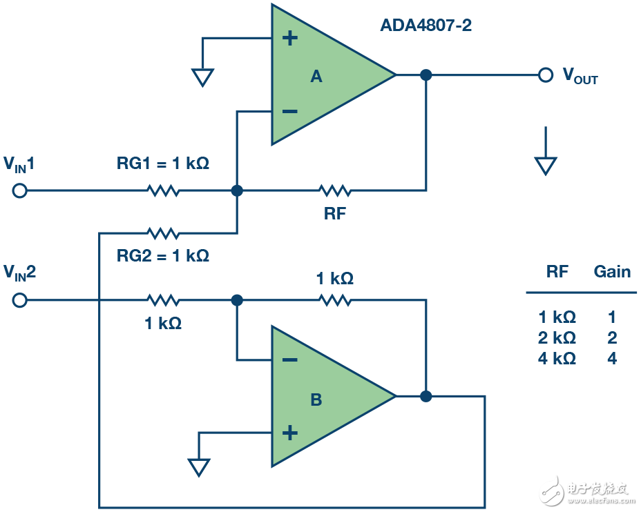
A simple solution is to use a two-channel precision amplifier with a resistive gain network, as shown in Figure 1. This circuit shows a simple way to convert a differential input to a single-ended output with adjustable gain. The system gain can be determined by Equation 1:
 |
Where gain = RF/1 k and (VIN1 – VIN2) is the differential input voltage.

Figure 1. Differential Input Single-Ended Output Amplifier
In general, this method provides a more stable read function in the presence of EMI or RFI, so it is recommended to use it in the presence of noise problems. This is especially true when measuring thermocouple, strain gauge and bridge pressure sensor inputs because they provide very small signals in noisy environments.
This circuit not only measures the voltage difference between the positive and negative terminals of the sensor, but also provides common-mode rejection with partial system gain for superior performance improvement over single-ended inputs. Furthermore, this sensor ground can also be different from the analog ground. The ground output voltage reference is very important in many applications. System accuracy depends on the tolerance of the network resistor.
The circuit converts the differential input to a single-ended output with adjustable gain. The system gain can be set by the ratio of RF to RG1, assuming RG2 = RG1 and amplifier B has a gain of -1.
For example, the 180 MHz dual amplifier ADA4807-2 can be built as an inverting amplifier for this application, and this circuit is less noisy. This circuit has a low quiescent current (1000 A/amplifier) ​​for low power, high resolution data conversion systems.
The input common mode voltage will be higher than the supply voltage. Rail-to-rail output is used, which is very useful in large common mode signals or large output voltage applications. For example, the data acquisition board has an ADC that accepts 0 V to 5 V single-ended inputs. However, the signal source happens to be the differential voltage generated by the sensor bridge, one terminal of the bridge is positive and the other terminal is negative in response to the pressure in the presence of common mode noise.

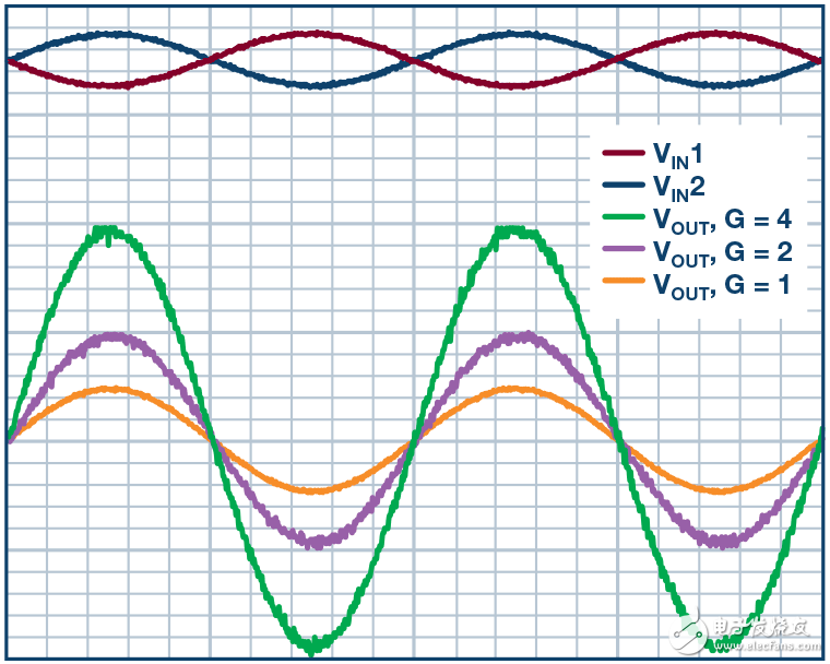
Figure 2. Performance of a differential-to-single-ended amplifier
Figure 2 shows the application of differential input voltage and circuit gain variation. The RF value sets the system gain. As you can see, this plot shows system gains 1, 2, and 4 with a differential input voltage of 1 V pp at 1 kHz.
This circuit is very useful for measuring small differences between two large voltages. For example, consider a solution that uses a 1% simple accuracy to monitor a typical Wheatstone bridge circuit powered by 3 V/GND in a 3 V battery-powered system. The required level of accuracy can be achieved with a 1% resistor or better, and this circuit will reject any common mode and amplify the attenuated bridge signal according to the set circuit gain. If the ADC is driven, some level shifting function is required to obtain an output signal in the 0 V to 5 V range.
The circuit features both excellent distortion and low quiescent current. Dual op amp solutions reduce system cost while differential amplifiers improve performance.
Ethernet Slip Ring is a device that allows Ethernet signals to be transmitted through a rotating assembly. This device is typically used in applications where it is not possible or practical to run Ethernet cables, such as in an application where the cables would have to travel through a hazardous area. It converts the regular Ethernet signals into rotary signals, which are then transmitted through the rotating assembly.
There is a growing trend in the industry for Ethernet slip rings. Ethernet slip rings are currently being used to interconnect computer networks. A slip ring is a transmission device that uses a counter-rotating encircling belt to transfer power and data between two or more devices.
Senripgrid Conductive Slip Ring has the following characteristics Direct unplugging of the RJ45 connector Upon reaching eight simultaneous ports, follow the standard cable connection method Work with either copper or gas-liquor joints Transmission to the external network (10M, 100M, 1Km Base T).
Ethernet Slip Ring,Generator Collector Rings,Through Bore Rotary Union,Rotary Pressure Joint
Dongguan Oubaibo Technology Co., Ltd. , https://www.sliprobs.com