With the development of communication technology, Gigabit Ethernet has become the first choice for high-speed transmission equipment due to its high bandwidth and high rate in transmission. Embedded system design based on Xilinx FPGAs integrates a range of intellectual property (IP) cores to make them powerful, enabling embedded serial Gigabit Ethernet development with FPGAs.
This design uses Xilinx's 65 nm process grade Virtex5 FXT series of chips to meet the high performance, high density, low power and low cost requirements of embedded system design. The V5 Hard TEMAC module provides dedicated Ethernet functionality and interfaces to the serial Gigabit Ethernet interface via the FPGA's internal high-speed serial transceiver GTX and Marvell's 88E1111 physical layer interface chip. The physical layer interface chip supports four Ethernet interface modes: MII, GMII, RGMII, and SGMII. Compared with the GMII interface, the SGMII interface has a small number of I/O ports, which facilitates PCB layout, and the data signals appear in the form of differential pairs, which is beneficial to ensure signal integrity [1].
This article combines the FPGA embedded PowerPC hard core processor, Xilinx thin embedded operating system Xilkernel, and the corresponding peripheral IP Core to complete the design of embedded serial Gigabit Ethernet.
1 overall designThe system hardware platform uses Xilinx's Virtex5 FX70t as the main control chip, which integrates the PowerPC440 processor module and the high-speed RockeTIO GTX transceiver.
The external memory uses Micron's 128M & TImes; 16-bit DDR SDRAM chip MT47H128M16HG 31T to provide space for program operation.
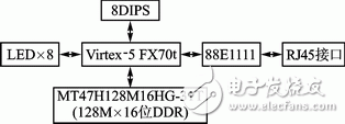
There are two options for the network chip, that is, the single physical layer chip solution and the physical layer plus the MAC layer are integrated in the same chip solution [2]. Based on ease of control considerations, Marvell's 88E1111 single physical layer interface chip is used as a solution that supports 10BASET, 100BASETX and 1000BASET Ethernet protocols. The system hardware consists of Virtex5 FX70t chip, 88E1111 PHY chip, DDRII chip, 8 DIP switches (8DIPS), 8 LED lights and RJ45 interface. The connection block diagram is shown in Figure 1.

Figure 1 system hardware connection block diagram
In the serial Gigabit Ethernet design, the FPGA internal RockeTIO GTX transceiver is required to complete the establishment of the SGMII link. RockeTIO GTX is a flexible, configurable, Gigabit-class serial transceiver integrated into the Virtex5 FX70t chip. It supports data rates from 750 Mbps to 6.5 Gbps and meets the data transfer rate requirements of Gigabit Ethernet system designs. This design completes the establishment of the SGMII link by instantiating the EMAC hard core in the FPGA and connecting the corresponding FPGA port to the external PHY chip 88E1111. The SGMII interface uses full-duplex mode. It has two independent channels for transmission and reception. Each channel uses a pair of differential signal lines. In the no-clock signal mode, the RocketIO GTX transceiver recovers the clock from the serial data for differential data transmission. receive.
The block diagram of the SGMII interface implementation is shown in Figure 2.

Figure 2 SGMII interface implementation block diagram
The system is based on Xilinx embedded system development tool EDK12.3 to complete the software and hardware collaborative design. EDK12.3 is composed of XPS (Xilinx Platform Studio), SDK (Software Development Kit), and the like. The design needs to add the required IP core in the XPS environment, generate the hardware system framework, add the corresponding pin constraints and timing constraints, and then call Platgen to generate the netlist (.NGC) files and bits of the hardware part of the embedded system ( .bit) file, and set the system software configuration through the software description file (.MSS file); then import the hardware design into the SDK, and generate the driver layer and library of each peripheral in the SDK, and set the operating system of the corresponding software. , library, peripheral driver properties, add application software projects and write application software; Finally, call the compiler corresponding to the compiler to compile the software and synthesize with the hardware executable file, generate the final binary bit file, download to the target board System debugging [3].
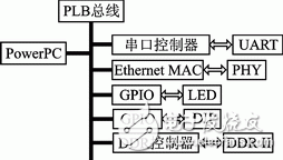
2 PowerPC hardware designThe FPGA embedded hard processor PowerPC440 used in the design is a 32-bit reduced instruction set embedded processor. It uses an extended BookE architecture, which includes a high-performance, dual-instruction processing and seven-stage pipelined microkernel. At the same time, it has a flexible memory management unit (MMU), three independent 128-bit PLB bus interfaces, four direct memory storage (DMA) control units, and a device control register (DCR) [4]. It integrates 32 KB instructions and 32 KB data cache to deliver up to 1 100 DMIPS at 550 MHz clock frequency. In this design, the PowerPC440 is connected to the peripheral port through the PLB bus, and its hardware architecture is shown in Figure 3.

Figure 3 Embedded System Hardware Architecture
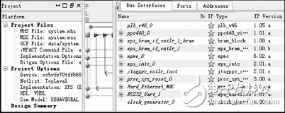
The construction of the system hardware platform (including PowerPC processor function configuration, system bus structure and corresponding address mapping) is completed in the EDK integrated development environment XPS.
In the design, the on-chip high-speed data bus PLB is used to connect various control IP cores. The PowerPC440 completes the access and control functions of the internal IP core and peripherals through the PLB bus. The external PHY chip is connected to the EMAC core (Ethernet MAC) inside the FPGA, and is mounted on the PLB bus to complete the establishment of the SGMII link; the DDR II chip passes the IP core multi-port memory controller (Multiport Memory Controller, MPMC) is mounted on the PLB bus to implement external storage function; the serial port is connected to the PLB bus through the serial port controller IP core (Xps_uartlite) for printout and output debugging status information; 8 DIP switches and LED lights pass through the GPIO port respectively. Connected to the PLB bus for simple control and status display.
The hardware structure is shown in Figure 4.

Figure 4 PowerPC hardware structure
Car Super Tweeter,Audio Car Tweeter,Car Tweeter Speakers,Audio Multimedia Driver
NINGBO BOILINGSOUND ELECTRONICS CO.,LTD , https://www.tweeterspeaker.com