When we conduct EMI analysis of electronic products or equipment, we must first analyze the propagation path of the system's interference; if there is an over-standard situation during our product design and testing, if we can solve the problem by analyzing the path or knowing the path of the interference source It has to be easy! In practical applications, I will summarize the coupling path of EMI-to provide a theoretical basis for the design!
EMI propagation path: inductive coupling; capacitive coupling; conduction coupling; radiation coupling!
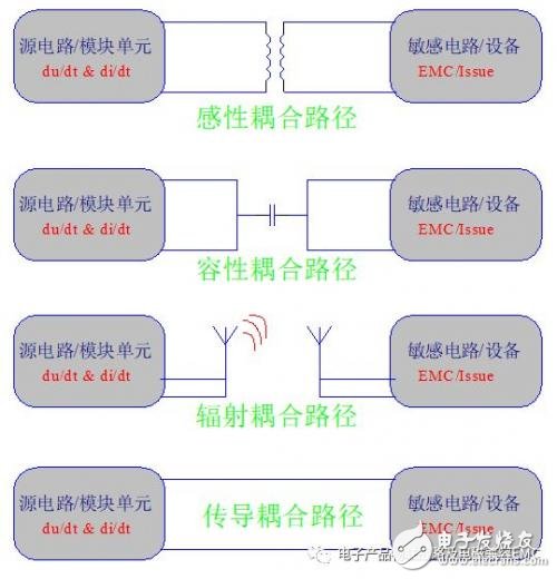
In electromagnetic compatibility design; our basic theory is: A. Confirm the noise source B. Understand the characteristics of noise sources C. Confirm the propagation path of the noise source; for the switching power supply system-"Switching Power Supply: EMC Analysis and Design", we have conducted a summary analysis of the noise source, and the three elements of electromagnetic compatibility are the key points;
The structure of the analysis block diagram is as follows:
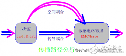
From the above three elements, we are familiar with the propagation path of EMI: spatial coupling and conduction coupling; we actually focus on using the above-mentioned theory for our practical guidance; in actual circuit design, our PCB design is also very good. The key: Basically 60% of EMC problems are PCB design problems. PCB design problems are limited by the product's PCB size & structure & the position of the interface will lead to the exception of EMC in our "Switching Power Supply: EMC Analysis and Design" problem!
The following paths of EMI conducted interference: (Total EMI coupling path) The analysis in the circuit is as follows:
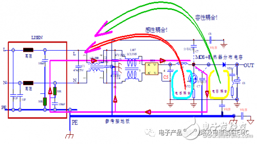
The above principle path schematic block diagram design provides a wide range of information, which can be extended to different power supply topologies; it involves system conduction theory and radiation theory; if the circuit is regarded as a standard PFC high-power application circuit; then you will Consider the harassment power of 30MHZ-300MHZ! If the front-stage input of the circuit structure is a low-voltage AC input (such as 12VAC), this circuit can be a standard boost (BOOST) circuit structure; change the position of the inductance, switch MOS and output diode; this circuit can become high-voltage or medium-voltage Low-voltage step-down (BUCK) circuit; that is to say, the application of this type of circuit can use the same equivalent structure in the performance and treatment of EMI problems; the problem of handling EMI is very similar.
A. In practice, we still have 10% EMI problem that many designers have not paid attention to! So we have to start with PCB analysis! ! The structure of the analysis block diagram is as follows:
1. Inductive coupling path problem

Pay attention to the inductive components in the circuit: inductors and transformers, etc.;
2. Capacitive coupling path problem

Note that any two similar current wires in the circuit will have distributed capacitive coupling: PCB traces and connecting wires, etc.;
B. The actual case appeared when I analyzed the special case; EMI conduction design-the optimization of the middle and high frequency part of our common mode filter has no obvious effect; the analysis block diagram structure is as follows:
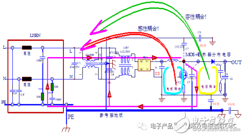
If the filter circuit of our EMI circuit uses a two-stage filter structure; when the size and structure of the common mode inductance, no matter how to adjust the test, it will not solve the EMI conduction problem of> 500KHZ-10MHZ; first pass the EMI path analysis; level 2 common mode The filter (common mode inductance and winding are OK!) is completely enough to solve the conduction interference of 150KHZ-10MHZ; the analysis is as follows:
1. Check the position of the inductance of the BUCK/BOOST (or PFC circuit) in the PCB design circuit from the input EMI filter; the loop area of ​​the high-voltage capacitor of the BUCK/BOOST circuit and the loop area of ​​the freewheeling diode, analyze and check whether the trace is close Input filter wiring! Perform basic PCB layout analysis! !
2. Use the simplest way to judge the problem; use a magnetic ring to wind the AC input power cord 3 times or more; EMI exceeding the standard point is immediately reduced or disappeared, and even passed the EMI test! ? analyze data! !
3. Through the verification of the magnetic ring above, it is obvious that we can find a way to solve the problem: remove the level 1 common mode inductance; use a two-wire parallel-wound common mode inductance (between 1-5mH) and place it at the power line entrance of the circuit board for testing ; Test whether the EMI test data reaches a margin above 5dB! So as to determine the problem;
After determining the EMI path of the system, optimize the PCB layout and routing of the circuit board according to my theory, and use the most optimized EMI filter structure to save a lot of design costs!
The layout of the following circuit board is a typical exception to the above design:
Test conduction data: 400K-3MHZ EMI conduction test data is very high!
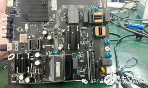
Checking according to the above 1, 2 and 3 also solved the EMI problem!
Gas Stove,Single Burner Gas Stove,Tempered Glass Panel Gas Stove,Stainless Steel Gas Stove
Shandong Sangle Group Co.,Ltd. , https://www.sangle-group.com