The rapid development of electronic technology puts higher requirements on electronic instruments and equipment: performance is more secure and reliable; function is increasing; in use, automation is getting higher and higher; in terms of volume, it is becoming smaller and smaller. This makes switching power supplies with many advantages increasingly used in computers, communications, aerospace, color TV and other aspects. However, in the switching regulator power supply, the switching transistor operates in the switching state, and its alternating voltage and current generate strong peak interference and resonance interference through the components of the circuit. These disturbances seriously pollute the utility grid, affecting the normal operation of nearby electronic instruments and equipment. At the same time, due to this shortcoming, the switching power supply cannot be applied to some sophisticated electronic instruments. Therefore, the electromagnetic interference of the switching power supply is minimized. To improve the scope of its use, it is a problem that must be considered in the design of switching power supplies.
In this paper, the principle of two-port network is applied, and the DC EMI filter in switching power supply is analyzed. The general method of DC EMI filter design and the calculation method of related parameters are given.
1 Design based on two-port network DC EMI filter
The widely used switching power supplies, whether single-bridge, push-pull, half-bridge, or full-bridge, can be summarized into the form shown in Figure 1 (in the case of a single phase).

Figure 1 General schematic of the switching power supply
It can be seen from Fig. 1 that by configuring the DC EMI filter, the equivalent impedance of the circuit can be changed to achieve the desired filtering effect.
The DC EMI filter dual port network model is shown in Figure 2. The mixed parameter equation is
![]() (1)
(1)
Where: g11 is the input admittance;
G22 is the output impedance;
G12 is the reverse current gain;
G21 is the forward voltage gain.

Figure 2 DC EMI filter dual port network model
A schematic diagram as shown in FIG. 3 can be equivalent to the equation (1).
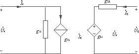
Figure 3 DC EMI filter equivalent schematic
The DC EMI filter design must meet the following requirements:
1) To ensure that the filter is filtered, it does not affect the load capacity of the power supply;
2) For the input DC component, the filter is required to not cause attenuation as much as possible;
3) For harmonic components, the filter should have a good filtering effect.
Combined with the mixed parameter equation and the equivalent schematic diagram, it is known from requirement 1) that the input admittance and output impedance of the filter should be as small as possible, ie g11=g22=0
According to requirement 2), at low frequencies, the design values ​​of the reverse current gain g12 and the forward voltage gain g21 should be as large as 1, while the input admittance and output impedance should be as small as possible, that is, g12=g21=1, g11=g22= 0;
According to requirement 3), at high frequencies, g11, g12, g21, and g22 should be as small as possible.
The above analysis conclusion is the general method of DC EMI filter design and the evaluation criteria of the filtering effect.
2 Case analysis
The LC filter and the fourth-order DC line filter are commonly used filters in engineering practice. The following conclusions are used to analyze the filtering effect. Figure 4 is a schematic diagram of the LC filter.

Figure 4 LC filter schematic
The mixed parameter equation is
(2)
For the DC component, since f tends to 0, corresponding to ω = 2πf tends to 0; obviously g11 = g22 = 0; g12 = g21 = 1.
For harmonic components,
|g11|= ![]() ;|g12|=
;|g12|= ![]() =|g21|;|g22|=
=|g21|;|g22|= ![]() .
.
Considering that when ωL>10, it is apparent that g11=g12=g21=g22=0. Analyze the input admittance and output impedance of the system, and ensure that the input admittance g11 tends to 0, which inevitably makes L take a large value; to ensure that the output impedance g22 tends to 0, the value of C must be made equally large, which gives the engineering actual Applications have limitations, which is a drawback of LC filters.
The schematic diagram of the fourth-order DC line filter widely used in engineering practice is shown in Fig. 5.
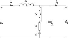
Figure 5 Schematic diagram of the fourth-order DC line filter
The mixed parameter equation is
(3)
In the formula:
g= ![]() .
.
If let z= ![]() , you can find the corresponding parameters as follows:
, you can find the corresponding parameters as follows:
G11=gz; g12=g21=z; g22=-L1sz.
The amplitude-frequency characteristic of the filter voltage transfer function is analyzed below, and the voltage transfer function of the filter is
G(s)= ![]() =
= ![]() (4)
(4)
Substituting the parameter g and applying MATLAB to make its logarithmic amplitude-frequency characteristic curve is shown in Fig. 6.
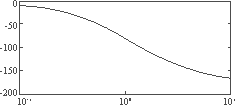
Figure 6 System amplitude frequency characteristic curve
Obviously, the attenuation of the output voltage in the low frequency band is small, and the filtering effect in the high frequency band is relatively obvious.
It can be seen from the above analysis that due to the wide selection of parameters of the circuit components, it is easier to design a filter that satisfies the design requirements and is suitable for engineering practice. The author has applied this circuit to a switching power supply designed for a company in Changsha.
The design requirements are:
1) Input a peak voltage of 1000V to generate a maximum of 20A;
2) When the filter output current changes from 0 to 25A, the 513V voltage fluctuation does not exceed 2%.
According to this design requirement, the design allowable values ​​are:
G11=20/1000=0.02;
G22=U/I=(513*2%)/25=0.4.
The final selected parameter values ​​are:
L1=500μH; L2=140μH; R0=0.3Ω;
C1 = 470 μF; C2 = 40 μF.
Substituting this set of parameter values ​​into equation (3) yields:
g=5; z=0.003;
G11=gz=0.015; g12=g21=0.003; g22=0.2.
The output voltage waveform of the switching power supply before and after adding this filter is shown in Figure 7.
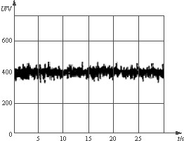
(a) Unfiltered power supply output waveform
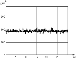
(b) Power output waveform after adding filter
Figure 7 switching power supply output waveform
3 Conclusion
This paper applies the two-port network principle, analyzes and summarizes the design requirements of the switching power supply EMI filter, and draws three design requirements, which is suitable for any filter design. From the design requirements, the performance of existing switching power supply EMI filters can be analyzed. In this paper, an EMI filter designed with this requirement is given and used in engineering practice. The running results show that the principle is both theoretical and practical, and has universality.
OVNS 1500 Puffs Vape is so convenient, portable, and small volume, you just need to take them
out of your pocket and take a puff, feel the cloud of smoke, and the fragrance of fruit surrounding you. It's so great.
We are the distributor of the ovns & vapeak vape brand, we sell ovns disposable vape,ovns vape kit, ovns juul compatible refillable pod, and so on.
We are also China's leading manufacturer and supplier of Disposable Vapes puff bars, disposable vape kit, e-cigarette
vape pens, and e-cigarette kit, and we specialize in disposable vapes, e-cigarette vape pens, e-cigarette kits, etc.
ovns 1500 puffs vape bars,ovns 1500 puffs vape device,ovns 1500 puffs vape disposable,ovns 1500 puffs vape starter kit,ovns 1500 puffs vape pen
Ningbo Autrends International Trade Co.,Ltd. , https://www.vapee-cigarettes.com