introduction
High availability systems such as servers, network switches, redundant arrays of disk arrays (RAID), and other forms of communications infrastructure require near-zero downtime throughout the life of the service. If a component of such a system fails or needs to be upgraded, it must be replaced without interrupting the rest of the system. If the system remains operational, the failed circuit board or module will be removed. Replacement parts are inserted. This process is called hot swapping (when the module interacts with the system software, it is also called hot plugging1). In order to achieve safe hot-swapping, connectors with staggered pins are usually used to ensure the establishment of ground and power before other connections, and in addition, in order to be able to easily remove and insert modules from the charged backplane, each block Hot-swappable controllers 2 are available on the printed circuit board (PCB) or hot-swap modules. In operation, the controller also provides continuous short-circuit protection and over-current protection.
Although the cut-off or opening current may be large, some of the subtleties of the high-current design are often not fully considered. "Details determine success or failure", this article will focus on analyzing the function and importance of each component in the hot-swap control circuit, and in-depth analysis of design considerations and device selection criteria when using ADI's ADM11773 hot-swap controller in the design process.
Hot swap technology
The two commonly used system supply voltages are -48 V and +12 V, and they use different hot plug protection configurations. The -48 V system contains the low-side hot-swap controller and the on-MOSFET; the +12 V system uses the high-end hot-swap controller and the on-MOSFET.
The -48 V scheme comes from traditional communication switching system technologies such as Advanced Communication Computing Architecture (ATCA) systems, optical networks, base stations, and blade servers. The 48 V power supply can usually be provided by the battery pack. The 48 V is selected because the power supply and the signal can be transmitted to a longer distance without suffering great loss. In addition, under normal conditions, the level is not high enough so it will not Serious electrical shock hazard. The reason for using a negative voltage is that when the device is inevitably exposed to a humid environment, the metal ions from the anode to the cathode are less corrosive when the positive pole is grounded.
However, in data communication systems, distance is not an important factor, and the +12 V voltage will be more reasonable. It is often used in servers and network systems. This article will focus on the +12 V system.
Hot plug event
Consider a system with a 12 V backplane and a set of removable modules. Each module must be removed and replaced without affecting the normal operation of any adjacent module. When there is no controller, each module may cause a large load capacitance on the power line, usually in the order of millimeters. When a module is first inserted, its uncharged capacitor requires all available current to charge it. If this inrush current is not limited, this large initial current will reduce the terminal voltage, causing the voltage on the main backplane to drastically drop, resetting multiple adjacent modules in the system, and damaging the module's connector.
This problem can be solved by the hot-swap controller (Figure 1). The hot-swap controller can reasonably control the inrush current and ensure the safe power-on interval. After power-on, the hot-swap controller can also continuously monitor the power supply current and avoid short circuits and over-current during normal operation.
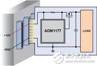
Figure 1 Hot Swap Application Block Diagram
Hot Swap Controller
The ADM1177 hot-swap controller includes three main components (Figure 2): an N-channel MOSFET that acts as a main switch for power control, a sense resistor that measures current, and a hot-swap controller. Hot-swap controllers are used to implement a loop that controls the MOSFET conduction current, which includes a current sense amplifier.
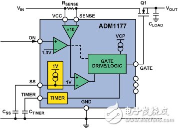
Figure 2, ADM1177 functional block diagram
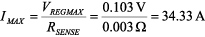
The hot-swap controller's internal current sense amplifier monitors the voltage drop across the external sense resistor. This small voltage (usually 0 to 100 mV) must be amplified to a usable level. The gain of the amplifier in the ADM1177 is 10, so, for example, a 100 mV voltage drop for a given current will be amplified to 1 V. This voltage will be compared with a fixed or variable reference voltage. If a 1V reference source is used, a current of more than 100 mV (±3%) on the sense resistor will cause the comparator to indicate overcurrent. Therefore, the maximum current trigger point depends mainly on the sense resistor, amplifier gain, and reference voltage; the sense resistor value determines the maximum current. The timer circuit is used to set the duration of the overcurrent.
The ADM1177 has a soft-start feature in which the over-current reference rises linearly, rather than abruptly turning on, which causes the load current to change in a similar manner. This can be achieved by injecting current from the internal current source to the external capacitor (SS pin), causing the reference input of the comparator to rise linearly from 0 V to 1 V. The external SS capacitor determines the speed of the rise. If needed, the SS pin can also be driven directly with voltage to set the maximum current limit.
An open circuit consisting of a comparator and a reference circuit is used to enable the device. It precisely sets the supply voltage that must be reached to enable the controller. Once the device is enabled, the gate begins to charge, and the gate voltage of the N-channel MOSFET used in this circuit must be higher than the source. In order to achieve this condition over the entire supply voltage (VCC) range, the hot-swap controller integrates a charge pump that maintains the GATE pin voltage at a level 10 V higher than VCC. If necessary, the GATE pin requires a charge pump pull-up current to enable the MOSFET and pull-down current is required to disable the MOSFET. The weaker pull-down current is used for regulation, and a stronger pull-down current is used to rapidly disable the MOSFET in the event of a short circuit.
The last basic module of a hot-swap controller is a timer, which limits the current adjustment time in case of overcurrent. The selected MOSFET can withstand a certain amount of power for the specified maximum time. MOSFET manufacturers use the diagram shown in Figure 3 to mark this range, or the Safe Operating Area (SOA).
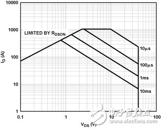
Figure 3 MOSFET SOA Diagram
The SOA diagram shows the relationship between the drain-source voltage, the drain current, and the duration that the MOSFET can withstand this power loss. For example, the MOSFET in Figure 3 can withstand 1 ms at 10 V and 85 A (850 W). If this condition lasts longer, the MOSFET may be damaged. The timer circuit uses an external timer capacitor to limit the time that the MOSFET experiences these worst-case conditions. For example, if the timer is set to 1ms, the circuit pauses and turns off the MOSFET when the duration of the current exceeds the 1ms limit.
To provide a safety margin, in the ADM1177, the timer's current-sensing voltage activation threshold is set to 92 mV, so the hot-swap controller starts timing when the sense voltage approaches 100 mV.
Design example
Since the design of the controller such as the ADM1177 allows for some flexibility, it is useful to demonstrate its application in the 12 V hot swap design example. In this example, assume:
The controller is ADM1177
VIN = 12 V (±10%)
VMAX = 13.2 V
ITRIP = 30 A
CLOAD = 2000 μF
VON = 10 V (better power on the controller)
IPOWERUP = 1 A (DC bias current required during power up)
To simplify the discussion, device tolerance effects are not considered in the calculations. Of course, these tolerances should be considered in the worst-case design.
ON pin
First consider the situation where the controller is enabled when the supply voltage exceeds 10 V. If the threshold of the ON pin is 1.3 V, the divider ratio from VIN to the ON pin should be set to 0.13:1. To ensure accuracy, the leakage of the pins should be taken into consideration when selecting the resistor.
The voltage divider ratio of a resistor divider consisting of 10 kΩ and 1.5 kΩ is 0.130.
Detection resistance selection
The selection of the sense resistor should be based on the load current required to start the timer.
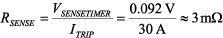
Where VSENSETIMER = 92 mV.
The maximum power consumed by the sense resistor at 30 A is
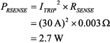
Therefore, the sense resistor should be able to withstand 3W of power. If there is no single resistor with the proper power rating or resistance, multiple resistors can be used in parallel to form the sense resistor.
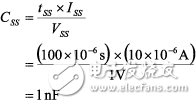
Load capacitor charging time
The time required to charge the load capacitor must be determined before selecting the MOSFET. During the power-up phase, the controller usually reaches the current limit due to the inrush current effect of the load capacitance. If the TIMER pin is not set to allow time for the load capacitor to charge, the MOSFET will be disabled and the system will not power up. We can use the following formula to determine the ideal charging time:
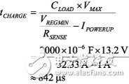
VREGMIN = 97 mV, which is the minimum adjustment voltage of the hot-swap controller.
This formula assumes that the load current rises from 0 A to 30 A instantaneously, which is an ideal case. In practice, the gate charge QGS of a larger MOSFET limits the slew rate of the gate voltage, thereby limiting the current, so a certain amount of charge is transferred to the load capacitor without triggering the timer function. In Figure 4, MOSFETs with larger QGS will cause the timer to operate shorter than MOSFETs with smaller QGS, the former being T1 ~ T3 and the latter being T0 ~ T2.
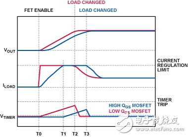
Figure 4. Influence of QGS during startup
This is because the increase in the transfer charge between T0 and T1 is less than the current limit, so the actual time is less than the time required for the calculation. This value is difficult to quantify and it depends on the controller gate current and the gate charge and capacitance of the MOSFET. In some cases, it may account for 30% of the total charging current, so it needs to be considered in the design, especially the design using large MOSFET and large current.
In the design of a MOSFET with a smaller gate charge, it can be assumed that the gate voltage rises quickly. This can lead to a rapid increase from 0 A to ITRIP, causing unwanted transients, in which case soft start should be used.
Soft start
With soft-start, the inrush current can increase linearly from zero to full-scale during the soft-start capacitor setting. By gradually increasing the reference current, the inrush current can suddenly reach the limit of 30 A. It should be noted that during the soft-start process, the current is in the process of adjustment. Therefore, the timer enters the working state from the beginning of soft start, as shown in Figure 5.
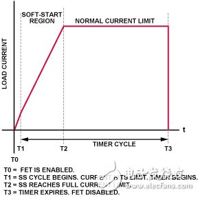
Figure 5 Effect of Soft Start on Timers
Therefore, it is recommended to set the soft start time to not exceed 10% to 20% of the total timer time. For example, 100 μs can be selected. The soft-start capacitance can be determined by the following formula:
ISS = 10 μA and VSS = 1 V.
MOSFET and Timer Selection
The first step in selecting the right MOSFET is to select the VDS and ID standards. For 12 V systems, VDS should be 30 V or 40 V to handle transients that can damage the MOSFET. The ID of the MOSFET should be much larger than the required maximum (refer to the SOA diagram in Figure 3). One of the most important indicators in high-current applications is the MOSFET's on-resistance RDSON. The smaller RDSON ensures that the MOSFET has minimal power consumption during normal operation and generates minimal heat at full load.
Heat and power considerations
Because overheating must be avoided, the power consumption of the MOSFET under DC load conditions should be considered before considering the SOA specifications and timer selection. As the MOSFET temperature increases, the rated power will be reduced or derated. In addition, the lifetime of the MOSFET is shortened when operating at high temperatures.
The previously mentioned hot-swap controller will start the timer with a minimum detection voltage of 92 mV. For the calculation, we need to know that the maximum allowable DC current of the timer will not be triggered. Assume that VREGMIN is 97 mV under worst-case conditions. Then,
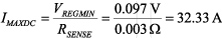
Assuming MOSFET's maximum RDSON is 2 mΩ, the power is
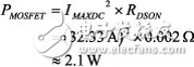
The data sheet will give the MOSFET thermal resistance at room temperature. The size of the package and the additional copper leads will have an impact on it. Hypothesis

Since the MOSFET needs to consume 2.1W of power, the temperature may rise to 126°C above room temperature in the worst case:
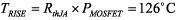
One way to reduce this value is to use two or more MOSFETs in parallel. This effectively reduces RDSON, which in turn reduces power dissipation in the MOSFET. When using two MOSFETs, the maximum temperature rise for each MOSFET is 32°C, assuming that the currents are evenly matched across the devices (allowing certain tolerances). The power consumption of each MOSFET is given by:
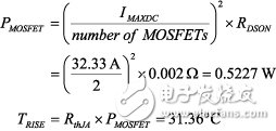
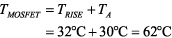
Assuming room temperature TA = 30°C, plus this temperature rise, the maximum temperature of each MOSFET is 62°C.
MOSFET SOA consideration
The next step is to check the SOA diagram to choose the right MOSFET that can work in the worst case. In the worst-case condition of short-circuit to ground, it can be assumed that VDS is equal to VMAX, which is 13.2V, which is the maximum voltage that the MOSFET can generate when the MOSFET source is pulled to ground. In the regulation phase, the worst case condition will depend on the maximum value of the hot-swap controller's regulation point in the data sheet. This value is 103 mV. Thus, the current can be calculated according to the following equation:
Before comparing with the MOSFET SOA diagram, we need to consider the temperature derating of the MOSFET because SOA is based on the data at room temperature (TC = 25°C). First calculate the power consumption at TC = 25°C:
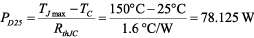
Among them RthJC can be got from MOSFET data sheet.
Now do the same calculation for TC = 62°C:
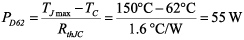
Therefore, the derating factor of 1.42 can be calculated as follows:
This needs to be applied to the MOSFET SOA diagram of FIG. In order to reflect the adjusted power rating, it is necessary to translate the diagonal line representing the time value at which the maximum power is applied. We first use the 1 ms line to illustrate the principle of this curve. For example, to take a point on this line, such as (20 A, 40 V), the power at this point is 800 W. Apply the derating formula:
At 40 V, the current corresponding to the derated power is 14 A. This point on the SOA chart will determine the new 1 ms line after the 62 °C derating. Use the same method to determine the new 10 ms and 100 μs lines. The new line is shown in red in FIG.
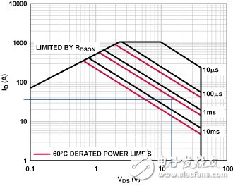
Figure 6. SOA diagram with power limit after derating at 62°C
Select timer capacitor
New derating lines in SOA can be used to recalculate timer parameter values. Draw a horizontal line along IMAX ≈ 35A, a vertical line (light blue line) along VMAX = 13.2 V, and determine their intersection with the red line. These intersections show some time between 1 ms and 10 ms, maybe 2 ms. In the small range of the logarithmic graph, it is generally difficult to obtain accurate values, so careful choices must be made, taking into account the impact of these choices on performance and other criteria such as price, to ensure that there are sufficient tolerances.
The previously mentioned charge time for the load is approximately 850 μs. Since the soft-start time is determined by the linear ramp, it takes longer time to charge the load capacitance than the step change. To estimate the total amount of charge, if soft-start is used, it is assumed that half of the soft-start time needs to be added to the calculation time. So, add half the soft-start time (50 μs) to 850 μs to get a total time of about 900 μs. If the selected MOSFET has a large gate charge (such as ≥80 nC), as described earlier, this time needs to be further reduced. If the time to charge the load is less than the maximum SOA time, the MOSFET is suitable. In this example, the MOSFET meets the standard (0.9 ms, 2 ms).
A timer value of less than 2 ms is sufficient to protect the MOSFET and greater than 0.9 ms is sufficient to charge the load. If you choose a constant time of 1 ms, the capacitance can be calculated by:
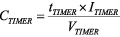
Where ITIMER = 60 μA and VTIMER = 1.3 V,
When using parallel MOSFETs, the calculation of the timer does not change. It is important to use a single MOSFET design timer and short-circuit protection, because in a set of MOSFETs, VGSTH will be significantly different, so in the adjustment process, you need to use a single MOSFET to handle the larger current.
Complete hot swap design
Figure 7 shows a parallel MOSFET hot-swap design with correct parameter values. The ADM1177 hot-swap controller also performs other functions. It integrates an on-chip ADC that can be used to convert supply voltage and load current to digital data for readout via the I2C bus, providing fully integrated current and voltage detection.
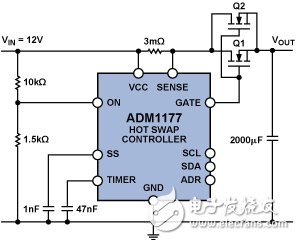
Figure 7. Complete reference design
Modular Plug,modular jack rj45,modular jack cat6,mod plugs
NINGBO UONICORE ELECTRONICS CO., LTD , https://www.uniconmelectronics.com