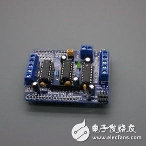
The HX711 is a 24-bit A/D converter chip designed for high-precision electronic scales. Compared with other chips of the same type, the chip integrates peripheral circuits required by other types of chips including a regulated power supply and an on-chip clock oscillator, and has the advantages of high integration, fast response, and strong anti-interference.
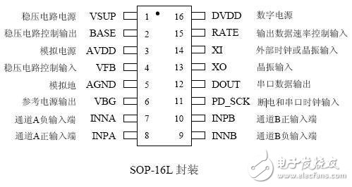
1, VSUP power regulator circuit power supply: 2.6 ~ 5.5V (AVDD should be connected when the regulator circuit is not needed)
2, BASE analog output regulator circuit control output (no connection when the regulator circuit is not used)
3, AVDD power analog power supply: 2.6 ~ 5.5V
4, VFB analog input voltage regulator circuit control input (should be grounded when no voltage regulator circuit is used)
5, AGND ground analog ground
6, VBG analog output reference power output
7, INA- analog input channel A negative input
8, INA + analog input channel A positive input
9, INB- analog input channel B negative input
10, INB+ analog input channel B positive input
11, PD_SCK digital input power-off control (active high) and serial clock input
12, DOUT digital output serial data output
13, XO digital input and output crystal input (no connection when crystal is not used)
14, XI digital input external clock or crystal input, 0: use on-chip oscillator
15, RATE digital input and output data rate control, 0: 10Hz; 1: 80Hz
16, DVDD power digital power: 2.6 ~ 5.5V
Analog inputThe Channel A analog differential input interfaces directly to the differential output of the bridge sensor. Since the signal output from the bridge sensor is small, in order to make full use of the input dynamic range of the A/D converter, the programmable gain of the channel is large, 128 or 64. These gains correspond to a full-scale differential input voltage of ±20mV or ±40mV, respectively.
Channel B is a fixed 64-gain with a corresponding full-scale differential input voltage of ±40mV. Channel B is applied to system parameter detection including batteries.
Power supplyThe digital power supply (DVDD) should use the same digital power supply as the MCU chip.
The regulator circuit in the HX711 chip provides analog power to both the A/D converter and external sensors. The regulated power supply voltage (VSUP) can be the same as the digital power supply (DVDD). The output voltage value (VAVDD) of the regulated power supply is determined by the external partial resistors R1 and R2 and the output reference voltage VBG of the chip (Fig. 1). VAVDD=VBG(R1+R2)/R2. The output voltage should be chosen to be at least 100mV below the regulated input voltage (VSUP). If the on-chip voltage regulator circuit is not used, pin VSUP and pin AVDD should be connected and connected to a low noise analog power supply with a voltage of 2.6 to 5.5V. No external capacitor is required on the pin VBG, the pin VFB should be grounded, and the pin BASE is no connection.
Clock selectionIf pin XI is grounded, the HX711 will automatically select the internal clock oscillator and automatically turn off the external clock input and the associated circuitry of the crystal. In this case, the typical output data rate is 10 Hz or 80 Hz.
If an accurate output data rate is required, connect the external input clock to the XI pin through a 20pF DC-blocking capacitor or connect the crystal to the XI and XO pins. In this case, the clock oscillator circuit inside the chip will automatically shut down.
The closed, crystal clock or external input clock circuit is used. At this time, if the crystal frequency is 11.0592 MHz, the output data rate is accurate 10 Hz or 80 Hz. The output data rate and the crystal frequency are proportionally increased or decreased in the above relationship. When using an external input clock, the external clock signal does not have to be a square wave. The clock signal on the crystal output pin of the MCU chip can be connected to the XI pin through a 20pF DC blocking capacitor as an external clock input. The amplitude of the external clock input signal can be as low as 150mV.
Serial communication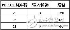
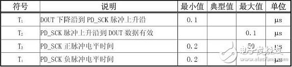
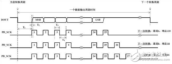
The serial communication line consists of pins PD_SCK and DOUT for outputting data and selecting the input channel and gain. When the data output pin DOUT is high, it indicates that the A/D converter is not ready for output data. At this time, the serial clock input signal PD_SCK should be low. When DOUT goes from high to low, PD_SCK should input 25 to 27 clock pulses. The rising edge of the first clock pulse will read out the most significant bit (MSB) of the 24-bit data until the 24th clock pulse is completed, and the 24-bit output data is output bit by bit from the highest bit to the lowest bit. The 25th to 27th clock pulses are used to select the input channel and gain for the next A/D conversion.
The number of input clock pulses of PD_SCK should not be less than 25 or more than 27, otherwise it will cause serial communication error.
When the input channel or gain of the A/D converter changes, the A/D converter requires 4 data output cycles to stabilize. DOUT will go from high level to low level after 4 data output cycles, and output valid data.
Hx711 data output, input channel and gain selection timing diagram
When the chip is powered up, the power-on automatic reset circuit in the chip will automatically reset the chip.
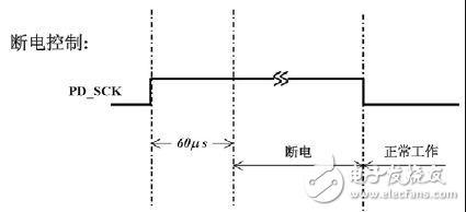
The pin PD_SCK input is used to control the power-down of the HX711. When PD_SCK is low, the chip is in normal operation.
If PD_SCK goes from low to high and stays high for more than 60μs, the HX711 enters a power-down state. If an on-chip regulated power supply circuit is used, the external sensor and the on-chip A/D converter will be powered off at the same time when the power is turned off. When PD_SCK returns to low level, the chip will automatically reset and enter normal operation. Chip from reset or power off state
After entering normal operation, channel A and gain 128 are automatically selected as the input channel and gain for the first A/D conversion. Subsequent input channels and gain selection are determined by the number of pulses in PD_SCK, see the Serial Communication section.
After the chip enters the normal working state from the reset or power-off state, the A/D converter needs four data output cycles to stabilize. DOUT will go from high level to low level after 4 data output cycles, and output valid data.
ZGAR AZ Vape Pods 5.0
ZGAR electronic cigarette uses high-tech R&D, food grade disposable pod device and high-quality raw material. All package designs are Original IP. Our designer team is from Hong Kong. We have very high requirements for product quality, flavors taste and packaging design. The E-liquid is imported, materials are food grade, and assembly plant is medical-grade dust-free workshops.
From production to packaging, the whole system of tracking, efficient and orderly process, achieving daily efficient output. WEIKA pays attention to the details of each process control. The first class dust-free production workshop has passed the GMP food and drug production standard certification, ensuring quality and safety. We choose the products with a traceability system, which can not only effectively track and trace all kinds of data, but also ensure good product quality.
We offer best price, high quality Pods, Pods Touch Screen, Empty Pod System, Pod Vape, Disposable Pod device, E-cigar, Vape Pods to all over the world.
Much Better Vaping Experience!


Pods, Vape Pods, Empty Pod System Vape,Disposable Pod Vape Systems
ZGAR INTERNATIONAL(HK)CO., LIMITED , https://www.zgarette.com