Improved synchronization method and realization of remote data collection based on GPS
It is often necessary to realize the synchronous collection of remote data in engineering. Most existing systems of this type adopt the method of "time stamping" the collected data to achieve synchronization of data collection. A large number of "data stamps" are stored in the RAM along with the data, occupying the RAM storage space and increasing the complexity of subsequent data processing. In response to the above problems, this paper proposes a level-triggered synchronization method. The main point is to use GPS timing to detect the arrival of the preset acquisition start time and generate a high-level trigger signal at the rising edge of the next second pulse at that time. , A group of data collection devices distributed in different places can therefore work synchronously. The specific system is designed according to the above method, and the experiment is carried out. The results show that the synchronization accuracy of 1 μs can be achieved [1].
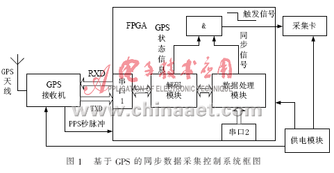
1 Synchronization principle and implementation scheme The NEMA information output by the GPS receiver is sent to the decoding module through the serial port 1, and the GPS status information and time information are extracted and output to the AND gate and data processing module, respectively. The data processing module processes the input time information and compares it with the preset time information input from serial port 2 every 1 s. If the two are completely the same, a synchronization signal is generated at the next rising edge time of the second pulse. When both the GPS status information and the synchronization signal level are high, a trigger signal is generated to trigger a group of remotely distributed data collection devices to start working synchronously.
For a group of data collection devices that need to be collected synchronously in different locations, each device adds one (FPGA) synchronization device, presetting the same collection start time. The synchronization device continuously detects the arrival of the time according to the GPS timing information, and triggers the data collection action at the rising edge of the next second pulse at the time, so that the data collection devices distributed in different places start to work synchronously.
The system block diagram of a single synchronization device is shown in Figure 1.
2 System hardware design
2.1 Introduction
2.1.1 GPS receiver performance brief introduction This system uses Navysyc CW25 receiver, this receiver is a specialized time receiver. The receiver has 12 parallel channels, can track 12 satellites at the same time, is fully calibrated to UTC time, produces synchronous timing with an accuracy of up to tens of nanoseconds, and supports RS-232 serial communication with a communication rate of 38 400 b / s.
2.1.2 Introduction of GPS second pulse output characteristics Second pulse PPS (Pulse Per Second) [5-6] is a level signal output in the form of a square wave with a period of 1 s and a high level duration of 100 μs. The rising edge of the high level is the precise moment of the PPS output, and its waveform is shown in Figure 2.
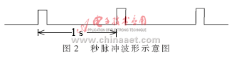
When the receiver achieves effective navigation, the difference between the pulse rising edge time and the UTC time is within ± 30 ns. The output of the UTC time in the RS-232 transmission data has a certain delay from the second pulse rising edge, that is, the receiver first provides the user with seconds Pulse, and then provide corresponding time information, (FPGA) synchronous control module must deal with this (lag of time information) properly, so that the rising edge of PPS corresponds to the actual time information.
2.2 Overall realization of system hardware The hardware design of this system mainly uses FPGA to design and realize synchronous control function. Since the serial communication between FPGA and GPS uses a standard RS-232 interface, the IP core provided by EDK can be directly implemented.
3 FPGA design
3.1 The top-level design uses FPGA to realize the core processing unit of the GPS-based remote data acquisition synchronous control system. It adopts a top-down design method and is described in Verilog HDL language. Xilinx Spartan-3A FPGA is used in simulation, synthesis and Realize [2-3]. The top-level design consists of the decoding module, I / O control module and data processing module.
The working process is: the serial port receives the NEMA $ POLYT statement from the GPS receiver, the I / O control module detects the start and end of the statement character, and checks the correctness of the statement format, and stores the correct statement in the input buffer; the decoding module Extract the time information and GPS positioning information from the NEMA information, input the time information into the data processing module, and input the GPS positioning information as an AND gate; in the data processing module, process and latch the time information sent by the decoding module, and The preset time information is compared. When the two are exactly the same, a synchronization signal is generated at the next rising edge of the PPS. This synchronization signal and the GPS positioning information are combined to generate a trigger signal to trigger the data acquisition card to start working synchronously.
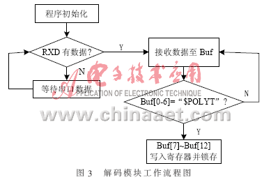
3.2 Decoding module The task of the decoding module is to extract the time information in the NEMA sentence sent by the GPS receiver. The serial port of the FPGA receives the NEMA $ POLYT statement from the GPS receiver. The I / O control module detects the start and end flag characters of the statement and checks the correctness of the statement format. The correct statement is stored in the input buffer and then from the buffer Extract time information and latch it. The format of the $ POLYT statement is as follows: $ POLYT, hhmmss.ss, ddmmyy, UTC_TOW, week, GPS_TOW, Clk_B, Clk_D, PG, cs, each item is separated by a comma, where the "hhmmss" item is the hour and minute of Greenwich Mean Time , Second information, FPGA control board can get the time information corresponding to 1 PPS signal by interpreting this message information [3]. The program flow chart of the decoding module works is shown in Figure 3.
3.3 Data processing module The function of the data processing module has two parts: adjust the time information extracted from the cache and generate a synchronous trigger signal.
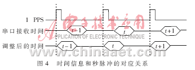
The adjustment time information includes two aspects. (1) The time output by the GPS receiver is GMT time, which needs to be converted to the time in the time zone where the current geographic location is located. (2) Since the time information of the GPS receiver is always sent from the serial port after the corresponding rising edge of the second pulse, so when the rising edge of the second pulse arrives at time t, the time information at time t has not yet been processed by the data processing unit received. In order to realize the synchronous output of the second pulse and time information, it is necessary to add 1 s to the time information at time t-1 as the absolute time at time t. Figure 4 shows the correspondence between the time before and after adjustment and the second pulse.
Compare the adjusted time information with the preset time information, the two are exactly the same. A level signal is generated at the corresponding time of the rising edge of the next PPS pulse. This signal and the GPS status information are "in phase with" and the output signal is the trigger signal of the data acquisition card. The simulation results are shown in Figure 5.

This paper presents an improved synchronization method of GPS-based remote data collection, and uses FPGA to carry out specific design and implementation. The experimental results show that the above method and design overcome the shortcomings of the commonly used "timestamp" method occupying extra storage space and increasing the burden of data processing, meeting the synchronization accuracy requirements of distributed data collection, and helping to achieve the miniaturization of synchronization devices , High stability, easy to maintain and upgrade.
64V Battery Pack ,Lithium Battery Box,Lithium Power Pack,Jackery Battery Pack
Zhejiang Casnovo Materials Co., Ltd. , https://www.casnovonewenergy.com