Abstract: This application note compares the serial and digital interfaces (SPI ™ or 3-wire, I²C or 2-wire) commonly used in two analog ICs. Each interface shows its advantages and disadvantages in different designs. It depends on the data rate, available design space, and noise environment. This application note gives the difference between the two interfaces and illustrates these points in detail with examples.
Introduction Although the signals in the real world are all analog signals, more and more analog ICs now use digital interfaces for communication. The data communication of the serial interface is between the master (providing a serial clock) and the slave / peripheral. Currently, most microcontrollers provide SPI (3-wire) and I²C (2-wire) interfaces for sending and receiving data. The microprocessor controls peripheral devices through several buses, such as: analog-to-digital converter (ADC), digital-to-analog converter (DAC), smart battery, port expansion, EEPROM, and temperature sensor. The difference from transmitting data through the parallel port is that the serial interface continuously transmits data through 2, 3, or 4 data / clock buses. Although the parallel interface has the characteristics of fast transmission speed, the serial interface occupies less control and data lines.
Basic knowledge of serial interface There are three kinds of serial interface: 3-wire, 2-wire and single wire. This article mainly discusses 3-wire and 2-wire serial interfaces. The serial peripheral interface (SPI), queue serial peripheral interface (QSPI ™) and MICROWIRE ™ (or MICROWIRE PLUS ™) interface standards all use a 3-wire interface. The inter-chip bus (I²C) and the system management bus (SMBus ™) are both 2-wire interfaces. These serial interfaces have their own advantages and disadvantages, as shown in Table 1.
3-wire interface The 3-wire interface uses chip select lines (active low CS or SS), clock lines (SCLK), and data input / host output lines (DIN or MOSI). The 3-wire interface sometimes also includes a data output / host input line (DOUT or MISO), which is also called a 4-wire interface. For simplicity of description, this article refers to 3-wire interface and 4-wire interface collectively as 3-wire interface.
The 3-wire interface can operate at a higher clock frequency and does not require a pull-up resistor. Both SPI / QSPI and MICROWIRE interfaces can work in full-duplex mode (data can be sent and received at the same time), generally working in noisy environments is not a problem. The 3-wire interface is edge-triggered, not level-triggered, so it has stronger anti-interference ability.
The main disadvantage of the 3-wire interface is that it provides a low-level CS line for each slave unless the slaves are connected in a daisy chain, as shown in Figure 1 (the daisy chain method will be discussed in detail in subsequent chapters). Another disadvantage is that the 3-wire interface does not have a response mechanism to judge whether the data is sent and received correctly. From the perspective of software design, in single-master / single-machine applications, the 3-wire interface is simpler and more efficient than the 2-wire interface.
Figure 1. A 3-wire interface for communication using data input, data output, clock, and chip select signals.
2-wire interface 2-wire interface includes a data line (SDA or SMBDATA) and a clock line (SCL or SMBCLK). The advantage of the 2-wire interface is that it uses fewer wires, which is especially important for compact designs, such as: mobile phones, fiber optic applications. Because the 2-wire interface assigns a unique address to each slave, multiple slaves can be connected on one bus without the need for chip select signals. The 2-wire interface transmits an acknowledge bit after successfully completing a read operation. Because the 2-wire interface has only one data line, it can only work in half-duplex mode (data reading and writing cannot be performed simultaneously). Because the 2-wire interface is level-triggered, if a data bit error occurs in a noisy environment, it may cause problems.
Table 1. Comparison of advantages and disadvantages of 3 / 2-wire interface
The master and slave communicate via a serial interface via multiple buses. During the write cycle, the master uses its own clock and data to transfer the data to the slave. During the read cycle, the slave transmits data to the master.
SPI, QSPI and MICROWIRE design The SPI interface developed by Motorola has been adopted by many popular processors and microcontrollers, such as the MAXQ2000. The SPI interface requires two control lines (active low CS and SCLK) and two data lines (DIN / SDI and DOUT / SDO). Motorola's SPI / QSPI standard calls the DIN / SDI data line as MOSI (master out, slave in), the DOUT / SDO data line as MISO (master in, slave out), and the CS line as SS (slave selection). In order to clarify the narrative, we explain the data line of the 3-wire interface based on the slave. DIN is the data input line of the slave, and DOUT is the data readout line of the slave. This article uses low-level active CS, SCLK, DIN, and DOUT to define each line in the 3-wire interface. Maxim peripherals use these pin names.
Most SPI interfaces have two configuration bits. The clock polarity (CPOL) and clock phase (CPHA) are used to set when the slave collects data. CPOL determines whether the bus is idle when SCLK is high (CPOL = 1) or when SCLK is low (CPOL = 0). CPHA decides on which edge of SCLK to move data in and out. When CPOL = 0, set CPHA to 0, indicating that the data is moved into the slave on the rising edge of SCLK; set CPHA to 1, indicating that the data is moved into the slave on the falling edge of SCLK. The two states of CPOL and CPHA allow four different combinations of clock polarity and phase. Each is incompatible with the other three. In order to achieve communication between the master and slave, the CPOL and CPHA of the master and slave must have the same settings.
In most applications of the SPI interface, the SPI interface transfers 8 bits of data (one byte) at a time, and some microprocessors transfer two or more bytes at a time. For example, the MAXQ2000 microprocessor can transmit 8-bit or 16-bit data at a time. When CPOL = 0 and CPHA = 0, the active low CS changes from high to low, starting a master to slave transmission process. During the eight cycles of high and low changes of the SCLK signal, the active low CS signal must be kept low. The DIN data is locked on the rising edge of the SCLK signal. In the same 8-bit period, the slave output data on the DOUT line is valid on every falling edge of SCLK. Figure 2a shows the detailed timing when CPHA = 1; Figure 2b shows the detailed timing when CPHA = 0.
Figure 2a. 3-wire interface timing (CPHA = 1), CPHA = 1, CPOL = 1, the 3-wire interface moves data into the peripheral on the rising edge of the clock and data out of the peripheral on the falling edge of the clock.
Figure 2b. 3-wire interface timing (CPHA = 0), CHPA = 0, CPOL = 1, the 3-wire interface moves data into the peripheral on the falling edge of the clock and data out of the peripheral on the rising edge of the clock.
Because each IC on the bus requires a dedicated chip select line, an active low CS is used as the enable signal for each slave. If there are four slaves on a bus, four chip select lines are needed. If the slave's active low CS is high (disabled), the slave ignores the data on the SCLK line and sets DOUT to high impedance.
Part of the 3-wire interface devices can be linked into a daisy chain without the need to provide low-level CS lines for each slave. The daisy-chain mode can use a low-level CS line and a data line to control multiple Tandem slave. In the daisy chain structure, the 3-wire interface must include the DOUT line. As shown in Figure 1, the DOUT of slave # 1 is connected to the DIN of slave # 2, and so on.
The maximum data rate is not defined in the SPI standard. The external device defines its own maximum data rate, usually in the order of MHz. The microprocessor can adapt to a wide range of SPI data rates. When using the SPI interface for communication, the slave cannot reduce the data rate of the master or determine an appropriate rate.
The QSPI standard is very similar to the SPI standard. In fact, peripherals cannot distinguish between the QSPI bus and the SPI bus. Unlike the host in the SPI standard, the host in QSPI allows data to be transferred through programmable chip select lines. The QSPI host can even transmit data between 8 and 16 bits in length, while the SPI host can only transmit 8-bit data. QSPI devices can be configured to continuously transmit data longer than 16 bytes (maximum 256 bits). This transmission is completely realized by the configuration of the QSPI device, without the operation of the MCU. Similar to the SPI interface, the QSPI interface does not specify a maximum data rate.
The old MICROWIRE standard developed by National Semiconductor is very similar to the SPI standard. The difference is that the clock polarity and clock phase of the MICROWIRE standard are fixed (CPOL = 0 and CPHA = 0). Data reading from DIN is always locked on the rising edge of SCLK. The data output of DOUT is always on the falling edge of SCLK. The MICROWIRE standard does not specify a maximum data rate.
The inter-chip circuit interface (I²C) is different from the full-duplex 3-wire interface. The I²C interface developed by Philips implements half-duplex communication through a data line (SDA) and a clock line (SCL). The I²C interface defines a simple master / slave bidirectional communication interface. In this system, the MCU decides whether it is the master (write mode) or the slave (receive mode). Each slave has a unique and unique address, so that the master can communicate with multiple slaves through a bus without the need to provide a separate chip select line for each slave. As shown in Figure 3, the number of slaves is limited only by the maximum line capacitance (400pF). The mechanism of the I²C interface is based on 7-bit or 10-bit addresses. 7-bit addresses are more common. In the 7-bit address mechanism, 127 different peripherals can be connected to the bus. The SCL and SDA lines have an open-drain structure, so they must be high when idle. When the power supply voltage is 3V, connect a pull-up resistor of 1kΩ or more; when the power supply voltage is 5V, connect a pull-up resistor of 1.6kΩ or more.
Figure 3. A 2-wire interface for communication using data input / output and clock signals.
When SCL is high, SDA changes from high to low, that is, a start command is issued to start I²C communication. As shown in Figure 4a, each SCL clock transmits one data bit, and at least 9 data bits are required to transmit one byte. A write cycle includes 8 data bits and an acknowledge bit (ACK) or non-acknowledge bit (NACK). As shown in Figure 4b, when data is transferred on the I²C bus, it is written to the slave on the rising edge of SLK and output from the slave on the falling edge of SLK. During the time when the SCL clock period is high, the data of the SDA line cannot be changed. The completion of a transmission must be followed by a command to abort or restart, that is, when SCL is high, SDA changes from low to high. When the bus is idle, both SDA and SCL are high.
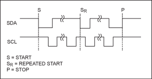
Figure 4a. Start condition and stop condition. The 2-wire interface uses start, repeat start and stop commands to transfer data between the master and slave.
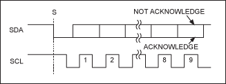
Figure 4b. I²C response bit. When responding to data, the 2-wire interface pulls SDA low.
The I²C write cycle begins with the start command, followed by the 7-bit slave address and the 8th bit used to identify read and write operations. Set the 8th position low to indicate a write operation; set the 8th position high to indicate a read operation. The host releases the bus after the 8th clock cycle. If the slave answers the data transmission, it will pull SDA low during the 9th clock cycle. If the slave does not answer the write command, the SDA is released (the data line is placed high through the pull-up resistor).
Subsequently, the host writes the 8-bit command byte, followed by the second ACK / NACK bit. Next, the host writes an 8-bit data byte and follows the third ACK / NACK bit. The data byte and the last acknowledge bit complete a read / write cycle and update the peripheral output. Figure 5a is a detailed example of a write cycle.
The I²C read cycle begins with the start command, followed by the slave address where data needs to be written, and the 8th position is high, indicating a read operation. After ACK / NACK, the master writes the command byte to access the slave register. After the second ACK / NACK bit, the master rewrites the slave address. After the third ACK / NACK bit, the slave controls the bus and outputs 8-bit data to the bus at a time. As shown in Figure 5b, when reading data from the same slave register as the last read operation, the master only needs to write the slave address before reading the slave data.
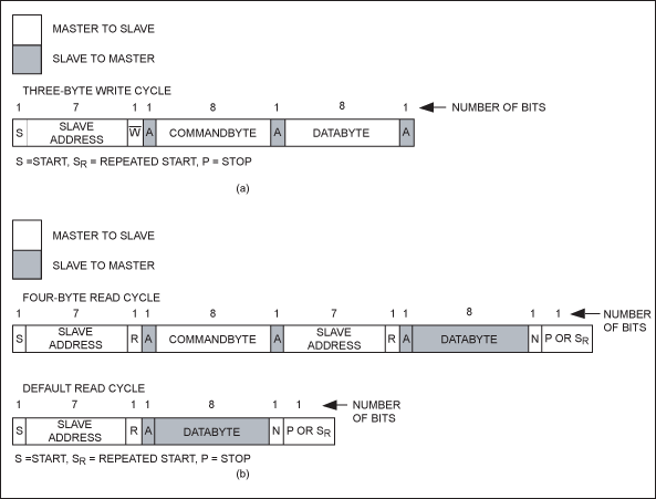
Figure 5. The 2-wire interface transmits 8 bits of data at a time. Figure 5a is an example of an I²C write cycle; Figure 5b is an example of an I²C read cycle.
The I²C interface supports three data rates: low speed (greater than 100kHz), fast (greater than 400kHz) and high speed (greater than 3.4MHz). The high and low levels of the I²C interface are CMOS logic levels (low level is below 0.3x power supply voltage and high level is above 0.7x power supply voltage).
System Management Bus (SMBus) Intel® has developed the SMBus standard for low-speed communication. The SMBus 2-wire interface is very similar to the I²C interface. SMBus also uses a data line (SMBDATA) and a clock line (SMBCLK) for communication. SMBCLK and SMBDATA also require pull-up resistors. The pull-up resistor is greater than 8.5kΩ when 3V power is supplied, and greater than 14kΩ when 5V power is supplied. SMBus operating voltage range is between 3V and 5V, higher than 2.1V is high level, lower than 0.8V is low level.
The main difference between the I²C interface and the SMBus interface is the highest / lowest clock rate. Because the I²C bus is a passive transmission bus, there is no bus timeout problem, and the rate can be as low as "stationary". The SMBus interface has a bus timeout problem. If the time after the clock signal is pulled down is greater than the timeout period (the longest is 35ms), the slave resets the interface and considers that a bus timeout has occurred. The SMBus timeout period limits the minimum clock rate to 19kHz. In order to ensure normal communication, the rate of SMBCLK must be between 10kHz and 100kHz, and the master or slave of the I²C interface can keep the clock at a low level according to the needs of transmitting data.
Examples of peripherals Microprocessors often communicate with peripherals through a serial interface. When a microprocessor accesses a peripheral through a 2-wire or 3-wire interface, the peripheral changes its analog or digital output accordingly. For example, it refers to setting the current and voltage for charging the battery, controlling the fan with a temperature sensor, and setting the analog output of the digital-to-analog converter.
As shown in Figure 6, a microprocessor and an 8-bit digital-to-analog converter (MAX5115) are connected through a 2-wire interface. Because this DAC has four address selection pins, it can generate 16 unique slave addresses, so 16 DACs can be connected in parallel on the bus, because MAX6641 has different slave addresses, the same 2-wire interface can also set the SMBus temperature Sensor / fan controller (MAX6641), the fan controller controls the gate of the MOSFET to turn the fan on or off.

Figure 6. Because the microcontroller uses an I²C interface, when communicating with peripherals such as DACs and temperature sensors, the bus only requires two wires.
The 3-wire interface requires a separate chip-select line to communicate between the microprocessor and multiple parallel slaves. The simpler 2-wire interface uses a clock line and a data line to communicate with each device on the bus. Multiple ICs can be connected to the bus by setting different slave addresses. Most I²C interface peripherals have address selection pins to implement slave address configuration. The number of slave addresses that the peripheral can use is equal to the square of the number of address selection pins. For example, if there are two address selection pins outside, it can be configured with four different addresses.
The new generation design provides more slave addresses with fewer address selection pins. The MAX7319 is an input / output expansion chip that can expand 16 slave addresses from two address selection pins (AD2 and AD0). These pins can be connected to GND, power supply (VCC), SDA or SCL. Table 2 lists the details of these 16 slave addresses. A6, A5, and A4 are fixed at 110, and A3 to A0 can be set by AD2 and AD0.
Table 2. The MAX7319 can compile 16 different addresses using only 2 address lines (AD2 and AD0)
There are several different requirements for further improvement of the 3-wire interface and 2-wire interface, and each interface has its own special advantages. In the near future, it is impossible to completely replace another interface standard with one interface standard. Devices with I²C interfaces have developed rapidly, and have begun to incorporate some of the features of SMBus interfaces, supporting functions such as timeout reset, so that the interface can be shut down as needed. The new I²C slave address is up to 10 bits, not just 7 bits, which gives users more flexibility.
The 3-wire interface and 2-wire interface will coexist, but the I²C interface seems to have a larger market share, and most microprocessors support 2-wire interfaces. The ease of use of the I²C interface and fewer connections make it grow more than the SPI interface.
For additional information, please refer to Application Note 3967: "Selecting a Serial Bus" and Application Note 3438: "Serial Digital Network".
Introduction Although the signals in the real world are all analog signals, more and more analog ICs now use digital interfaces for communication. The data communication of the serial interface is between the master (providing a serial clock) and the slave / peripheral. Currently, most microcontrollers provide SPI (3-wire) and I²C (2-wire) interfaces for sending and receiving data. The microprocessor controls peripheral devices through several buses, such as: analog-to-digital converter (ADC), digital-to-analog converter (DAC), smart battery, port expansion, EEPROM, and temperature sensor. The difference from transmitting data through the parallel port is that the serial interface continuously transmits data through 2, 3, or 4 data / clock buses. Although the parallel interface has the characteristics of fast transmission speed, the serial interface occupies less control and data lines.
Basic knowledge of serial interface There are three kinds of serial interface: 3-wire, 2-wire and single wire. This article mainly discusses 3-wire and 2-wire serial interfaces. The serial peripheral interface (SPI), queue serial peripheral interface (QSPI ™) and MICROWIRE ™ (or MICROWIRE PLUS ™) interface standards all use a 3-wire interface. The inter-chip bus (I²C) and the system management bus (SMBus ™) are both 2-wire interfaces. These serial interfaces have their own advantages and disadvantages, as shown in Table 1.
3-wire interface The 3-wire interface uses chip select lines (active low CS or SS), clock lines (SCLK), and data input / host output lines (DIN or MOSI). The 3-wire interface sometimes also includes a data output / host input line (DOUT or MISO), which is also called a 4-wire interface. For simplicity of description, this article refers to 3-wire interface and 4-wire interface collectively as 3-wire interface.
The 3-wire interface can operate at a higher clock frequency and does not require a pull-up resistor. Both SPI / QSPI and MICROWIRE interfaces can work in full-duplex mode (data can be sent and received at the same time), generally working in noisy environments is not a problem. The 3-wire interface is edge-triggered, not level-triggered, so it has stronger anti-interference ability.
The main disadvantage of the 3-wire interface is that it provides a low-level CS line for each slave unless the slaves are connected in a daisy chain, as shown in Figure 1 (the daisy chain method will be discussed in detail in subsequent chapters). Another disadvantage is that the 3-wire interface does not have a response mechanism to judge whether the data is sent and received correctly. From the perspective of software design, in single-master / single-machine applications, the 3-wire interface is simpler and more efficient than the 2-wire interface.
Figure 1. A 3-wire interface for communication using data input, data output, clock, and chip select signals.
2-wire interface 2-wire interface includes a data line (SDA or SMBDATA) and a clock line (SCL or SMBCLK). The advantage of the 2-wire interface is that it uses fewer wires, which is especially important for compact designs, such as: mobile phones, fiber optic applications. Because the 2-wire interface assigns a unique address to each slave, multiple slaves can be connected on one bus without the need for chip select signals. The 2-wire interface transmits an acknowledge bit after successfully completing a read operation. Because the 2-wire interface has only one data line, it can only work in half-duplex mode (data reading and writing cannot be performed simultaneously). Because the 2-wire interface is level-triggered, if a data bit error occurs in a noisy environment, it may cause problems.
Table 1. Comparison of advantages and disadvantages of 3 / 2-wire interface
| Interface | Advantages | Disadvantages |
| 3-Wire: SPI, QSPI, and MICROWIRE PLUS | 1. Speed 2. No pullup resistors required 3. Full-duplex operaTIon 4. Noise immunity | 1. Larger number of bus line connecTIons 2. Individual chip-select lines required to communicate with more than one slave at a TIme 3. No acknowledgment of received data |
| 2-Wire: I²C and SMBus | 1. Fewer bus line connecTIons 2. Multiple devices share the same bus 3. Received data is acknowledged | 1. Speed: SMBus limited to 100kHz; I²C limited to 3.4MHz 2. Half-duplex operation 3. Open-drain bus lines require pullup resistors 4. Reduced noise immunity |
The master and slave communicate via a serial interface via multiple buses. During the write cycle, the master uses its own clock and data to transfer the data to the slave. During the read cycle, the slave transmits data to the master.
SPI, QSPI and MICROWIRE design The SPI interface developed by Motorola has been adopted by many popular processors and microcontrollers, such as the MAXQ2000. The SPI interface requires two control lines (active low CS and SCLK) and two data lines (DIN / SDI and DOUT / SDO). Motorola's SPI / QSPI standard calls the DIN / SDI data line as MOSI (master out, slave in), the DOUT / SDO data line as MISO (master in, slave out), and the CS line as SS (slave selection). In order to clarify the narrative, we explain the data line of the 3-wire interface based on the slave. DIN is the data input line of the slave, and DOUT is the data readout line of the slave. This article uses low-level active CS, SCLK, DIN, and DOUT to define each line in the 3-wire interface. Maxim peripherals use these pin names.
Most SPI interfaces have two configuration bits. The clock polarity (CPOL) and clock phase (CPHA) are used to set when the slave collects data. CPOL determines whether the bus is idle when SCLK is high (CPOL = 1) or when SCLK is low (CPOL = 0). CPHA decides on which edge of SCLK to move data in and out. When CPOL = 0, set CPHA to 0, indicating that the data is moved into the slave on the rising edge of SCLK; set CPHA to 1, indicating that the data is moved into the slave on the falling edge of SCLK. The two states of CPOL and CPHA allow four different combinations of clock polarity and phase. Each is incompatible with the other three. In order to achieve communication between the master and slave, the CPOL and CPHA of the master and slave must have the same settings.
In most applications of the SPI interface, the SPI interface transfers 8 bits of data (one byte) at a time, and some microprocessors transfer two or more bytes at a time. For example, the MAXQ2000 microprocessor can transmit 8-bit or 16-bit data at a time. When CPOL = 0 and CPHA = 0, the active low CS changes from high to low, starting a master to slave transmission process. During the eight cycles of high and low changes of the SCLK signal, the active low CS signal must be kept low. The DIN data is locked on the rising edge of the SCLK signal. In the same 8-bit period, the slave output data on the DOUT line is valid on every falling edge of SCLK. Figure 2a shows the detailed timing when CPHA = 1; Figure 2b shows the detailed timing when CPHA = 0.
Figure 2a. 3-wire interface timing (CPHA = 1), CPHA = 1, CPOL = 1, the 3-wire interface moves data into the peripheral on the rising edge of the clock and data out of the peripheral on the falling edge of the clock.
Figure 2b. 3-wire interface timing (CPHA = 0), CHPA = 0, CPOL = 1, the 3-wire interface moves data into the peripheral on the falling edge of the clock and data out of the peripheral on the rising edge of the clock.
Because each IC on the bus requires a dedicated chip select line, an active low CS is used as the enable signal for each slave. If there are four slaves on a bus, four chip select lines are needed. If the slave's active low CS is high (disabled), the slave ignores the data on the SCLK line and sets DOUT to high impedance.
Part of the 3-wire interface devices can be linked into a daisy chain without the need to provide low-level CS lines for each slave. The daisy-chain mode can use a low-level CS line and a data line to control multiple Tandem slave. In the daisy chain structure, the 3-wire interface must include the DOUT line. As shown in Figure 1, the DOUT of slave # 1 is connected to the DIN of slave # 2, and so on.
The maximum data rate is not defined in the SPI standard. The external device defines its own maximum data rate, usually in the order of MHz. The microprocessor can adapt to a wide range of SPI data rates. When using the SPI interface for communication, the slave cannot reduce the data rate of the master or determine an appropriate rate.
The QSPI standard is very similar to the SPI standard. In fact, peripherals cannot distinguish between the QSPI bus and the SPI bus. Unlike the host in the SPI standard, the host in QSPI allows data to be transferred through programmable chip select lines. The QSPI host can even transmit data between 8 and 16 bits in length, while the SPI host can only transmit 8-bit data. QSPI devices can be configured to continuously transmit data longer than 16 bytes (maximum 256 bits). This transmission is completely realized by the configuration of the QSPI device, without the operation of the MCU. Similar to the SPI interface, the QSPI interface does not specify a maximum data rate.
The old MICROWIRE standard developed by National Semiconductor is very similar to the SPI standard. The difference is that the clock polarity and clock phase of the MICROWIRE standard are fixed (CPOL = 0 and CPHA = 0). Data reading from DIN is always locked on the rising edge of SCLK. The data output of DOUT is always on the falling edge of SCLK. The MICROWIRE standard does not specify a maximum data rate.
The inter-chip circuit interface (I²C) is different from the full-duplex 3-wire interface. The I²C interface developed by Philips implements half-duplex communication through a data line (SDA) and a clock line (SCL). The I²C interface defines a simple master / slave bidirectional communication interface. In this system, the MCU decides whether it is the master (write mode) or the slave (receive mode). Each slave has a unique and unique address, so that the master can communicate with multiple slaves through a bus without the need to provide a separate chip select line for each slave. As shown in Figure 3, the number of slaves is limited only by the maximum line capacitance (400pF). The mechanism of the I²C interface is based on 7-bit or 10-bit addresses. 7-bit addresses are more common. In the 7-bit address mechanism, 127 different peripherals can be connected to the bus. The SCL and SDA lines have an open-drain structure, so they must be high when idle. When the power supply voltage is 3V, connect a pull-up resistor of 1kΩ or more; when the power supply voltage is 5V, connect a pull-up resistor of 1.6kΩ or more.
Figure 3. A 2-wire interface for communication using data input / output and clock signals.
When SCL is high, SDA changes from high to low, that is, a start command is issued to start I²C communication. As shown in Figure 4a, each SCL clock transmits one data bit, and at least 9 data bits are required to transmit one byte. A write cycle includes 8 data bits and an acknowledge bit (ACK) or non-acknowledge bit (NACK). As shown in Figure 4b, when data is transferred on the I²C bus, it is written to the slave on the rising edge of SLK and output from the slave on the falling edge of SLK. During the time when the SCL clock period is high, the data of the SDA line cannot be changed. The completion of a transmission must be followed by a command to abort or restart, that is, when SCL is high, SDA changes from low to high. When the bus is idle, both SDA and SCL are high.
Figure 4a. Start condition and stop condition. The 2-wire interface uses start, repeat start and stop commands to transfer data between the master and slave.
Figure 4b. I²C response bit. When responding to data, the 2-wire interface pulls SDA low.
The I²C write cycle begins with the start command, followed by the 7-bit slave address and the 8th bit used to identify read and write operations. Set the 8th position low to indicate a write operation; set the 8th position high to indicate a read operation. The host releases the bus after the 8th clock cycle. If the slave answers the data transmission, it will pull SDA low during the 9th clock cycle. If the slave does not answer the write command, the SDA is released (the data line is placed high through the pull-up resistor).
Subsequently, the host writes the 8-bit command byte, followed by the second ACK / NACK bit. Next, the host writes an 8-bit data byte and follows the third ACK / NACK bit. The data byte and the last acknowledge bit complete a read / write cycle and update the peripheral output. Figure 5a is a detailed example of a write cycle.
The I²C read cycle begins with the start command, followed by the slave address where data needs to be written, and the 8th position is high, indicating a read operation. After ACK / NACK, the master writes the command byte to access the slave register. After the second ACK / NACK bit, the master rewrites the slave address. After the third ACK / NACK bit, the slave controls the bus and outputs 8-bit data to the bus at a time. As shown in Figure 5b, when reading data from the same slave register as the last read operation, the master only needs to write the slave address before reading the slave data.
Figure 5. The 2-wire interface transmits 8 bits of data at a time. Figure 5a is an example of an I²C write cycle; Figure 5b is an example of an I²C read cycle.
The I²C interface supports three data rates: low speed (greater than 100kHz), fast (greater than 400kHz) and high speed (greater than 3.4MHz). The high and low levels of the I²C interface are CMOS logic levels (low level is below 0.3x power supply voltage and high level is above 0.7x power supply voltage).
System Management Bus (SMBus) Intel® has developed the SMBus standard for low-speed communication. The SMBus 2-wire interface is very similar to the I²C interface. SMBus also uses a data line (SMBDATA) and a clock line (SMBCLK) for communication. SMBCLK and SMBDATA also require pull-up resistors. The pull-up resistor is greater than 8.5kΩ when 3V power is supplied, and greater than 14kΩ when 5V power is supplied. SMBus operating voltage range is between 3V and 5V, higher than 2.1V is high level, lower than 0.8V is low level.
The main difference between the I²C interface and the SMBus interface is the highest / lowest clock rate. Because the I²C bus is a passive transmission bus, there is no bus timeout problem, and the rate can be as low as "stationary". The SMBus interface has a bus timeout problem. If the time after the clock signal is pulled down is greater than the timeout period (the longest is 35ms), the slave resets the interface and considers that a bus timeout has occurred. The SMBus timeout period limits the minimum clock rate to 19kHz. In order to ensure normal communication, the rate of SMBCLK must be between 10kHz and 100kHz, and the master or slave of the I²C interface can keep the clock at a low level according to the needs of transmitting data.
Examples of peripherals Microprocessors often communicate with peripherals through a serial interface. When a microprocessor accesses a peripheral through a 2-wire or 3-wire interface, the peripheral changes its analog or digital output accordingly. For example, it refers to setting the current and voltage for charging the battery, controlling the fan with a temperature sensor, and setting the analog output of the digital-to-analog converter.
As shown in Figure 6, a microprocessor and an 8-bit digital-to-analog converter (MAX5115) are connected through a 2-wire interface. Because this DAC has four address selection pins, it can generate 16 unique slave addresses, so 16 DACs can be connected in parallel on the bus, because MAX6641 has different slave addresses, the same 2-wire interface can also set the SMBus temperature Sensor / fan controller (MAX6641), the fan controller controls the gate of the MOSFET to turn the fan on or off.
Figure 6. Because the microcontroller uses an I²C interface, when communicating with peripherals such as DACs and temperature sensors, the bus only requires two wires.
The 3-wire interface requires a separate chip-select line to communicate between the microprocessor and multiple parallel slaves. The simpler 2-wire interface uses a clock line and a data line to communicate with each device on the bus. Multiple ICs can be connected to the bus by setting different slave addresses. Most I²C interface peripherals have address selection pins to implement slave address configuration. The number of slave addresses that the peripheral can use is equal to the square of the number of address selection pins. For example, if there are two address selection pins outside, it can be configured with four different addresses.
The new generation design provides more slave addresses with fewer address selection pins. The MAX7319 is an input / output expansion chip that can expand 16 slave addresses from two address selection pins (AD2 and AD0). These pins can be connected to GND, power supply (VCC), SDA or SCL. Table 2 lists the details of these 16 slave addresses. A6, A5, and A4 are fixed at 110, and A3 to A0 can be set by AD2 and AD0.
Table 2. The MAX7319 can compile 16 different addresses using only 2 address lines (AD2 and AD0)
| Pin Connection | Device Address | |||||||
| AD2 | AD0 | A6 | A5 | A4 | A3 | A2 | A1 | A0 |
| SCL | GND | 1 | 1 | 0 | 0 | 0 | 0 | 0 |
| SCL | VCC | 1 | 1 | 0 | 0 | 0 | 0 | 1 |
| SCL | SCL | 1 | 1 | 0 | 0 | 0 | 1 | 0 |
| SCL | SDA | 1 | 1 | 0 | 0 | 0 | 1 | 1 |
| SDA | GND | 1 | 1 | 0 | 0 | 1 | 0 | 0 |
| SDA | VCC | 1 | 1 | 0 | 0 | 1 | 0 | 1 |
| SDA | SCL | 1 | 1 | 0 | 0 | 1 | 1 | 0 |
| SDA | SDA | 1 | 1 | 0 | 0 | 1 | 1 | 1 |
| GND | GND | 1 | 1 | 0 | 1 | 0 | 0 | 0 |
| GND | VCC | 1 | 1 | 0 | 1 | 0 | 0 | 1 |
| GND | SCL | 1 | 1 | 0 | 1 | 0 | 1 | 0 |
| GND | SDA | 1 | 1 | 0 | 1 | 0 | 1 | 1 |
| VCC | GND | 1 | 1 | 0 | 1 | 1 | 0 | 0 |
| VCC | VCC | 1 | 1 | 0 | 1 | 1 | 0 | 1 |
| VCC | SCL | 1 | 1 | 0 | 1 | 1 | 1 | 0 |
| VCC | SDA | 1 | 1 | 0 | 1 | 1 | 1 | 1 |
The 3-wire interface and 2-wire interface will coexist, but the I²C interface seems to have a larger market share, and most microprocessors support 2-wire interfaces. The ease of use of the I²C interface and fewer connections make it grow more than the SPI interface.
For additional information, please refer to Application Note 3967: "Selecting a Serial Bus" and Application Note 3438: "Serial Digital Network".
Dash Cam For Honda,Wireless Dual Dash Cam,Dash Cam Front Rear And Inside,Honda Crv Dash Cam
SHENZHEN ROSOTO TECHNOLOGY CO., LTD. , https://www.rdtkdashcam.com