SPI (Serial Peripheral Interface);
I2C (INTER IC BUS)
UART (Universal Asynchronous Receiver Transmitter: Universal Asynchronous Receiver)
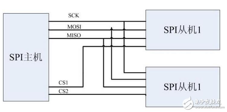
Second, the difference is on the electrical signal line:The SPI bus consists of three signal lines: serial clock (SCLK), serial data output (SDO), and serial data input (SDI). The SPI bus allows multiple SPI devices to be connected to each other. The SPI device that provides the SPI serial clock is the SPI master or master (Master), and the other devices are SPI slaves or slaves (Slave). Full-duplex communication can be achieved between master and slave devices. When there are multiple slave devices, a slave device selection line can also be added.
If you use the general-purpose IO port to simulate the SPI bus, you must have an output port (SDO), an input port (SDI), and the other port depends on the type of device implemented. If you want to implement a master-slave device, you need an input port. If only the master device is implemented, the output port is required. If only the slave device is implemented, only the input port is required.
The I2C bus is a bidirectional, two-wire (SCL, SDA), serial, multi-master (mulTI-master) interface standard with a bus arbitration mechanism that is ideal for close-range, non-recurring data communication between devices. In its protocol system, when the data is transmitted, the device address of the destination device is carried, so that the device networking can be implemented.
If the I2C bus is simulated with a general-purpose IO port and bidirectional transmission is required, an input/output port (SDA) is required, and an output port (SCL) is required. (Note: I2C data is less well understood, and the description here may be incomplete)
The UART bus is an asynchronous serial port, so it is generally much more complicated than the structure of the first two synchronous serial ports. Generally, the baud rate generator (the generated baud rate is equal to 16 times the transmission baud rate), the UART receiver, and the UART transmitter. The composition consists of two wires on the hardware, one for sending and one for receiving.
Obviously, if you use the general-purpose IO port to simulate the UART bus, you need an input port and an output port.
Third, it can be clearly seen from the second point that SPI and UART can achieve full duplex, but I2C does not work. Fourth, look at the opinions of the cattle people!Wudanyu: I2C line is less, I think it is more powerful than UART, SPI, but technically more troublesome, because I2C needs to have bidirectional IO support, and use pull-up resistor, I think the anti-interference ability is weak, generally used Communication between chips on the same board is less used for long-distance communication. The SPI implementation is simpler. The UART requires a fixed baud rate, which means that the two bits of data are equally spaced, and the SPI does not matter because it is a clocked protocol.
Quickmouse: I2C is a bit slower than SPI. The protocol is a bit more complicated than SPI, but the connection is less than the standard SPI.
SPI interface introduction (transfer)These days I encountered the flash using the SPI interface, only to know that the flash can also be serial. It seems that it was really a frog at the bottom of the well. I found some information about the SPI interface. I found a little English information and translated it. My personal understanding, made up an article, I hope to help a little beginner.
The full name of the SPI interface is "Serial Peripheral Interface", which means serial peripheral interface, which Motorola first defined on its MC68HCXX series processor. The SPI interface is mainly used in EEPROM, FLASH, real-time clock, AD converter, and between digital signal processor and digital signal decoder.
The SPI interface is synchronous serial data transmission between the CPU and the peripheral low-speed device. Under the shift pulse of the master device, the data is transmitted bit by bit, the high bit is in the front, the status is in the rear, the full-duplex communication, the data transmission speed is overall. It is faster than the I2C bus and can reach several Mbps.
The SPI interface operates in master-slave mode. This mode usually has one master device and one or more slave devices. The interface includes the following four signals:
(1) MOSI – master device data output, slave device data input
(2) MISO – master device data input, slave device data output
(3) SCLK – clock signal generated by the master device
(4) / SS – Slave enable signal, controlled by the master
![]()
In point-to-point communication, the SPI interface does not require addressing operations and is full-duplex communication, which is simple and efficient.
In a system with multiple slaves, each slave requires a separate enable signal, which is slightly more complicated on hardware than the I2C system.

![]()
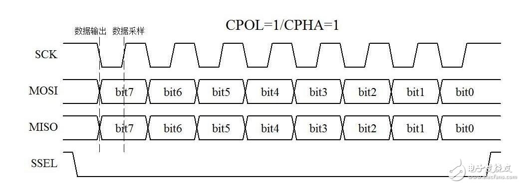
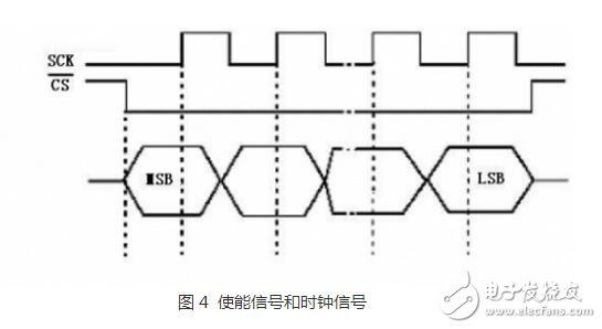
The SPI interface is actually two simple shift registers in the internal hardware. The transmitted data is 8 bits. It is transmitted bit by bit under the slave enable signal and shift pulse generated by the master device. The high bit is in the front and the low bit is in the back. . As shown in the figure below, the data changes on the falling edge of SCLK, and one bit of data is stored in the shift register.
![]()
Internal hardware representation of the SPI interface: (see below)
![]()
Finally, one drawback of the SPI interface is that there is no flow control specified and no response mechanism confirms receipt of the data.
Detailed analysis of the SPI serial bus connection method:The SPI bus system is a synchronous serial peripheral interface that allows the MCU to communicate serially with various peripherals to exchange information. It is because of the way of communication that we can control a wide variety of peripheral devices through the chip to achieve a lot of "unbelievable" modern technology. Here we will introduce the SPI bus from a programming perspective with the SPI title.
1. Introduction to SPI protocolSPI is an abbreviation for English Serial Peripheral interface, which, as its name suggests, is a serial peripheral interface. Motorola was first defined on its MC68HCXX family of processors. SPI is a high-speed, full-duplex, synchronous communication bus. Due to its easy-to-use features, many of the nor flash and nandflash chips now integrate this communication protocol, which is what we call SPI flash.
SPI flash chip is widely used, and it has more or less traces on many electronic products, such as mobile phones, digital, liquid crystal displays, set-top boxes, computer motherboards, etc. Recently, it was revealed that Apple's new mobile phone iPhone 8 will be introduced with coded flash memory (NOR Flash), which makes the NOR chip that is already out of stock more annoyed. According to the storage industry, this year's NOR chip supply gap will be possible. Expand to 20%.
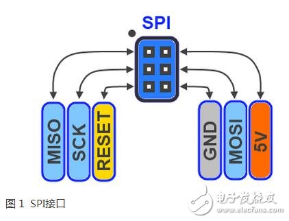
The SPI interface typically uses 4 lines of communication, MISO master data input, and slave device data output. MOSI master device data output, slave device data input. The SCLK clock signal is generated by the master device. The CS slave selects the signal and is controlled by the master.

The SPI interface generates the slave enable signal and the clock signal under Master control, and the two bidirectional shift registers perform bit-by-bit transmission for data exchange, and the transmission data is high and the low bit is (MSB). The data changes on the falling edge of SCK, and one bit of data on the rising edge is stored in the shift register.
After understanding the SPI protocol, let Xiaobian take you to easily operate the SPI flash chip. The operation of the flash chip generally includes the erasing, programming and reading of the flash chip. The SPI flash chips of all major manufacturers are similar, and the operation commands are basically unchanged. When we get a chip, we must pay special attention to the chip. The capacity, operation partition, the following takes Wang Hong's chip as an example for everyone to explain.
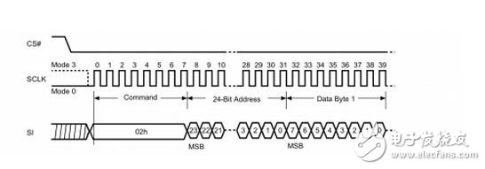
In fact, whether it is the chip erase, programming or read operation, we can roughly follow the following routine: write command --- write address --- write (read) data. As the following timing diagram is as clear and clear, we first pull the chip select signal low, then send a 0x02 page programming command, and then send an address, you can easily write data.
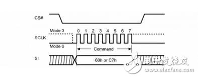
According to the sample hoist, the erase operation is the same, even simpler, but we should pay attention to the WIP bit of the loop judgment status register until the completion of the erase, the specific cycle time depends on the chip.
In addition, we must pay special attention to the OTP area of ​​SPI flash, that is, (ONE TIME PROGRAMMABLE), that is to say, this area can only be programmed once, and can not be modified and erased after programming, so we must pay special attention when operating. Before reading and writing to the OTP area, we must first send a command to enter the OTP area. The other operations are the same as those of the above normal flash area.
Mastering the above methods, we can easily operate the SPI flash chip. Of course, for the underlying operation of timing, we need to continuously learn and accumulate.
Antenk MICRO USB :Micro USB is a miniaturized version of the Universal Serial Bus (USB) interface developed for connecting compact and mobile devices such as smartphones, MP3 players, GPS devices, photo printers and digital cameras.
Micro USB connectors exist or have existed in three forms: micro A, micro B and micro USB 3. USB 3 micro is much like micro B, but with an additional pin group on the side for twice the wires, enabling USB 3's greater speed. Like standard USB, the micro versions are plug-and-play and hot-swappable.
Micro Usb2.0 B Female,Micro Usb SMT Dip,Usb SMT Dip with Flange,Micro Usb B Female SMT Dip
ShenZhen Antenk Electronics Co,Ltd , https://www.coincellholder.com