In the IC layout design, in addition to embodying the logic or function of the circuit to ensure correct LVS verification, it is necessary to add some graphics that are independent of LVS (circuit matching) to reduce the deviation in the intermediate process. We usually call these graphics a dummy layer. .
Use of dummy layer:1, to ensure manufacturability, to prevent the chip in the manufacturing process due to exposure transition or insufficient etching failure: such as tapeout will check the density of the chip, insert dummy metal, dummy poly, dummy diff, etc.;
2. Avoid the influence of the reflection and diffraction of light in the lithography process on the accuracy of the physical pattern of the key components, and affect the size: such as the resistors on the analog circuit and the dummy res and dummy caps on the periphery of the capacitor array, and Add dummy MOS, etc. near the key MOS;
3. Avoid the influence of noise on the key signal in the chip. Add dummy rouTIng layer around the key signal. The dummy component: if for some susceptible signal lines, in addition to minimizing the length of the trace, Dummy metal/poly should be added to the left and right of the trace and grounded to ensure that it is not affected by noise. Adding a dummy cap to the periphery of the cap also has a similar effect.
Dummy graphics in CMOS device layouts:1, MOS dummy
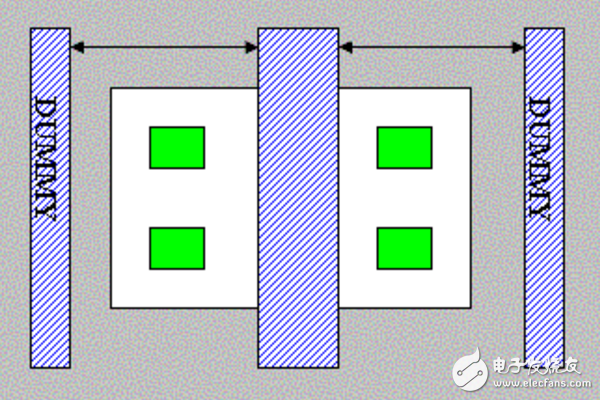
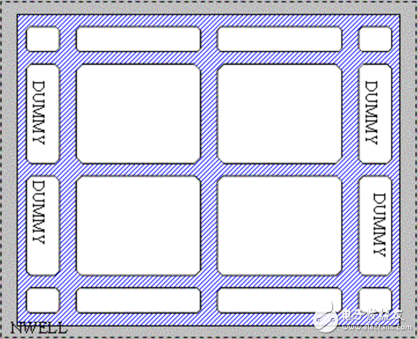
Add dummy poly on both sides of MOS to prevent Length from being affected. Connect VSS to the NMOS first, then add N type guard ring to connect VDD. Add NAND to PMOS first to connect VDD, then add P type to connect VSS. The split MOS should be an even root, and the Source end is connected to the surrounding guar ring. For example, the split NMOS is an even number, and the end connected to the VSS is on the outside and directly connected to the surrounding guard ring.
2, RES dummy
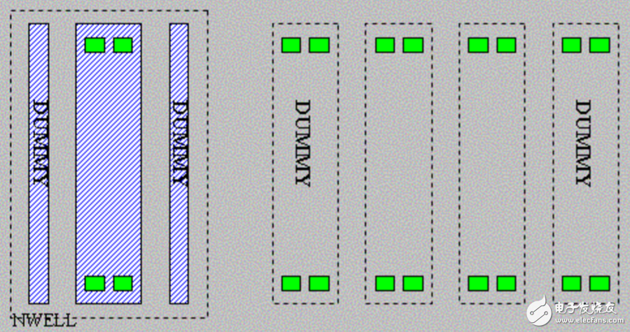
Similar to the MOS dummy method, the dummy is added, and it is sometimes added around. Adding nwell below the poly/diff resistor mitigates the effect of noise on the resistance, and nwell connects the high potential to the sub-bias. The Nwell resistor is surrounded by sub cont to connect to VSS. In order to reduce the effect of the resistance of the resistor, the Nwell resistor covers the metal and is connected to a high potential. Followed by a margin sufficient for the nwell resistor, usually nwell width 5-6um.
3, CAP dummy
Adding the dummy method is similar, using Nwell to block the phase from the substance, Nwell is connected to the high potential and the sub-bias.
4. The key traces and the shields of the left and right or upper and lower traces are processed by the same layer or intermediate layer connected to VSS.
Multiple Beam Angles street lights,LED Street light,Led White Light Street lamp
Kindwin Technology (H.K.) Limited , https://www.szktlled.com