Field Programmable Gate Arrays (FPGAs) are found in the heart of numerous prototypes and low to medium volume products. The main advantages of FPGAs are flexibility in the development process, a simple upgrade path, faster time to market, and relatively low cost. One major drawback is complexity, and FPGAs often incorporate advanced system-on-chip (SoC).
This complexity makes demanding requirements on the power supply. To meet these challenges, the power supply requires a combination of several output and switching regulator efficiencies and clean power of the linear regulator.
Computing system power supply
The powered FPGA looks like a complete system powered. Power supply design engineers face the challenge of 3 to 15 voltage rail supply (and sometimes even more); this is just the beginning. FPGAs are commonly manufactured using the latest wafer fabrication techniques that require low core voltages, but the power supply must also supply multiple rail special blocks and circuits, provide multiple voltage levels, supply additional current to high power modules, and satisfy noise sensitive components. Requirements.
Just to make things more complicated, even the same manufacturer of FPGAs can make a big difference, making it important that engineers choose the best power source for each chip. Such choices depend on a variety of factors, such as voltage and power requirements for each rail, rail 'sequencing requirements, and the need for power management of the system.
The first step in designing an FPGA power supply is to determine the individual voltage rails and their requirements. FPGA vendors typically provide a "pin" that specifies the voltage level at which each supply pin is connected to the device's voltage rail.
The FPGA's tracks are powered at several different voltages depending on the block being powered. Requirements usually include the core (powered internal logic array), I/O (driving the I/O buffers can be grouped in the bank, from each operation of a different voltage), phase-locked loop (PLL) (powered PLL core), as well as transceivers (send digital and analog circuits in transceivers, receivers and transmitters).
Once the personal voltage rail has been determined, the next step is to calculate the current consumption in turn on each track. At present, the lottery shared track should be added to the railway in the analysis, the total railway. Online calculators usually provided by FPGA vendors are used for this purpose. Next, engineers should add up all the power consumption of the components that make up the FPGA to accurately estimate the power consumption of the entire chip.
After calculating the power consumption, the next step is to check the specification voltage variation tolerance and the maximum voltage ripple for each track. These parameters can usually be found in the data sheets in the FPGA.
The output of the voltage regulator within the range determined by the load regulation specification (in mV) may deviate from the load. A typical gauge load is adjusted to ±5 mV if the power supply is derived from a switched DC-DC voltage converter ("switching regulator"). This is just one if the 0.4% deviation of the specified voltage rail at 1.2 V
The voltage ripple is measured from peak to peak in mV, and its size dependent voltage regulator provides the design of the particular track being analyzed. Output filtering severely affects voltage-(current) ripple performance. (See the Tech Zone article "Capacitor Selection Is Key, Designed with Good Voltage Regulators.") Most FPGAs withstand up to 2% or rail voltage, which is well within the capabilities of very modern switching regulators. Voltage ripple.
Switch or linear regulator?
The next step in the FPGA power supply design process is to determine if a particular track should be powered by a switching regulator or linear regulator. Of particular note is the analog power rail for noise sensitive circuits such as PLLs and transceiver circuits. Excessive noise on these rails can jeopardize the performance of the circuit.
The linear regulator provides ripple-free power, has a fast response, is simpler to use, and takes less space than a switching device. They are a good choice for noise sensitive PLL and transceiver rails. The main drawback is the lack of efficiency, especially when the output voltage is much lower than the input.
Switching regulators with high power rails, their higher efficiency than noise is more important and a better choice. They are a good choice for digital core logic and I power supply / FPGA, where the current requirements can be easily run to tens of amps of O operation. The disadvantage of a switching regulator is that it is more complex, bulky, and requires more external components. (See the Tech Zone article "Understanding the Advantages and Disadvantages of Linear Regulators.")
The resulting power supply can be a bit complicated, including several switching regulators and linear regulators in the "Power Tree" (Figure 2).
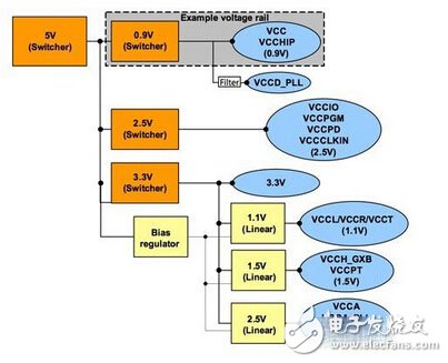
Figure 1: FPGA Power Supply with Switch and Linear Regulator
Nantong Boxin Electronic Technology Co., Ltd. , https://www.ntbosen.com