An integrated circuit, which belongs to PLD, has a large circuit scale.
CPLD refers to a programmable logic device with a relatively complex structure, which includes the following output macro cell structures:
Programmable I/O allows the user to program these pins as input or output.
Register outputs and feedback can be used to implement counters, shift registers, and more.
Exclusive OR gate output structure can be used for general user multi-function counting, which can effectively build large counters.
AMD first produced PAL22V10, a programmable logic device with macro cells. At present, PAL22V10 has become the demarcation line of PLD. The number of gates included in a programmable logic device is greater than the number of gates included in PAL22V10, and it is considered to be a complex programmable logic device (CPLD).
CPLD can be considered as basically an extension of the original programmable logic device. It is often composed of functional blocks of programmable logic around a central, time-delay fixed programmable interconnect matrix. Because the interconnection between the logic cells is realized by a fixed length of metal wire, and the programmable logic cells are similar to the PAL and the array, the CPLD and the FPGA can easily calculate the input delay from the input to the output. Obviously there will be Some flexibility restrictions. However, CPLD designs are simpler than FPGAs.
Although the structure of CPLDs is generally similar, and it is generally believed that CPLDs have a 100% pass rate, there may actually be differences due to the different structures of the interconnectable matrix.
CPLD is an abbreviation of Complex PLD. As its name suggests, CPLD is a complex logic element that is more complex than PLD.
CPLD is a highly integrated logic element. Due to its highly integrated nature, it has the advantages of improved performance, increased reliability, reduced PCB area, and reduced cost. CPLD components are basically a combination of many Logic Blocks. Each logic block is similar to a simple PLD element (such as 22V10). The interrelationships between the logic blocks are formed by a changeable link architecture that synthesizes the entire logic circuit.
Common CPLD components are Altera's Max5000 and Max7000 series. Cypress's Max340 and Flash370 series, in general, the gate count of CPLD components is about 1000~7000 Gate.
As the functionality of mobile phones and other portable handheld devices continues to increase, the trade-offs between designs have become increasingly sophisticated. Popular features such as text messaging and web browsing require more data entry, which is more difficult with traditional dual tone multi-frequency (DTMF) (0-9, #, *) keyboards. Using this type of keyboard requires multiple data inputs, which are inefficient and error-prone.

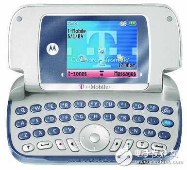
Figure 1 - QWERTY Keyboard (Motorola A630)
One way to make text input more convenient is to use the QWERTY keyboard (see Figure 1). This keyboard uses 40 or more keys, while the DTMF phone usually uses 12 keys. Of course, the extra buttons will make the phone bigger and use more electronic components.
However, text information users may be willing to trade QWERTY keyboards for volume because text input is much easier and both thumbs can be used to enter text messages or data. Recently, some mobile phone manufacturers have already launched text-enabled mobile phones with QWERTY keyboards.
The data input keyboard can be designed in a variety of ways without any restrictions. Adding more buttons to a traditional DTMF keyboard poses a challenge for designers, and this article discusses one possible solution to this challenge.
QWERTY building blockOur solution uses Xilinx® CoolRunnerTM-II CPLDs; its low power, small package, and low cost make it an ideal choice for this application.
Converting DTMF to a QWERTY keyboard requires more buttons, requiring more general purpose I/O (GPIO). For example, a DTMF keyboard may have only four rows and three columns, whereas a QWERTY keyboard may have up to eight rows and eight columns. However, the size of the keyboard may depend on the needs of the end system.

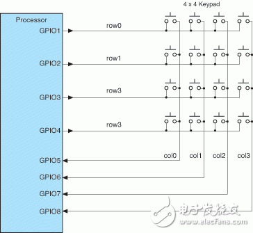
Figure 2 - Simple 4 x 4 Keyboard Connected to Processor Needs 8 GPIOs
Typically, a processor or DSP is used as the interface for connecting keyboard rows and columns (see Figure 2). The processor scans the rows and monitors the columns to detect logic changes. When the change occurs, the user presses a key. Knowing which line was scanned and which column's state has changed, the processor can infer which button was pressed.
Extended I/OWhen designing a keyboard that requires more I/O (a QWERTY keyboard is an example), you may find that your existing processor does not have enough GPIO. One possible solution is to use a CPLD as an I/O expander to reduce the number of processor I/Os.
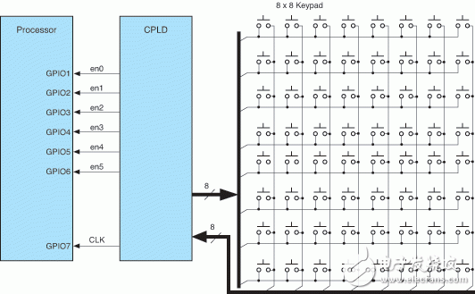
Figure 3 uses a CPLD between the processor and the keyboard, with one side connected to the row/column of the keyboard and the other side connected to the available GPIO of the processor. In this example, using a CPLD, an 8 x 8 keyboard requires the same number of processor GPIO ports as the 4 x 4 keyboard (in fact, one less). If you do not use a CPLD, the processor will need 16 GPIO ports instead of 7.
Scanning and encodingIn addition to reducing the number of GPIOs required by the processor, the CPLD can also assume certain functions of the processor, such as scanning rows and monitoring columns to detect state changes. When the user presses the key, the CPLD stops scanning and immediately generates a codeword that is sent to the processor to tell the processor which key was pressed. Because the encoded word is used to tell the processor which button was pressed, the processor's I/O requirements are reduced.

Figure 3 - Extended GPIO Using CoolRunner-II CPLDs
In the example shown in Figure 3, 6 bits are used to represent code words. The 6 bits provide 26 (or 64) different values, each representing a key press. However, there must also be a value that indicates when no button is pressed. Therefore, in this case, only 63 keys can actually be represented without adding another GPIO.
The processor does not need to scan the keyboard because the operation is now performed by the CPLD; however, the processor still needs to monitor the changes on its GPIO - it just no longer needs to infer which key was pressed because the information is encoded into a six-bit word. .
Also needed is switch jitter, which can be arranged in the CPLD or in the processor, depending on which device has available resources. Performing this operation in the processor minimizes the size and cost of the CPLD.
To briefly summarize this design example: The CPLD scans the keyboard, detects the pressed key, and then provides an encoded word for the processor to read and parse. This feature not only frees the processor from scanning tasks, but also extends GPIO functionality.
This design is ideal for the CoolRunner-II 32 macrocell unit (approximately 75% utilization), leaving 25% free for other uses. In addition, this design uses other methods to reduce power consumption and take advantage of CoolRunner-II's energy-saving features.
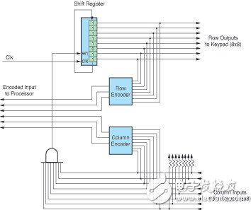
CPLD design detailsTo scan the keyboard's line, the barrel shift register is preset to 1 except that one bit is preset to zero. Each bit of the shift register drives an output pin on the CPLD, which is connected to the row of the keyboard. When the shift register starts timing, the zero bits are shifted by the barrel shifter and the row is de-asserted row by row to scan it. The column of the keyboard is input to the CPLD and each input is pulled up by an internal pull-up resistor.
When no key is pressed, all column inputs of the CPLD are passively pulled up to logic high. The AND operation is performed on all the column inputs together. The logic 1 on the output indicates that no key is pressed.
The output of the AND operation is used to start the shift register. When the key is pressed, the column and row get connected, and the column in which the key is pressed is set low by the row associated with the key. The output of the AND operation will become zero, which will abort the shift register when the key is pressed.

Figure 4 - Module Diagram
At this point, the shift register lowers the row where the key was pressed, and the column in which the key is located is also low. To correlate this information, two encoders are used: one for the row bit (output of the shift register) and one for the column input. The outputs of the two encoders are combined to form the codeword sent to the processor. Figure 4 is a block diagram of this operation.
ConclusionUsing the Xilinx CoolRunner-II CPLD, you get smart design and low power consumption. In addition to the I/O expansion, CPLDs can also incorporate other “bonding†functions such as voltage conversion, I/O standard conversion, and input hysteresis.
Because the CPLD is programmable, you can use the same device for different keyboards and products, resulting in higher yields and lower costs. The reprogrammability features are complemented by easy-to-use design tools that allow you to make late-stage changes to the design and reduce risk.
Smart Terminals,Smart Pos Terminal,Smart Pos Machine,Smartpay Terminal
Guangzhou Winson Information Technology Co., Ltd. , https://www.barcodescanner-2d.com