In terms of sampling rate and available bandwidth, today's radio frequency analog-to-digital converters (RF ADCs) have made considerable progress. It also incorporates a large number of digital processing functions, and the complexity of the power supply has also increased. So, why do RF ADCs today have so many different power rails and power domains?
In order to understand the growth of power domains and power supplies, we need to trace the history of ADC. As early as when the ADC was not high enough, the sampling speed was very slow, about tens of MHz, and the digital content was very small and almost nonexistent. The digital part of the circuit mainly involves how to transmit data to the digital receiving logic-application-specific integrated circuit (ASIC) or field programmable gate array (FPGA). The geometry of the process nodes used to manufacture these circuits is relatively large, about 180 nm or larger. Using a single voltage rail (1.8 V) and two different domains (AVDD and DVDD, for the analog domain and the digital domain, respectively), sufficient performance can be obtained.
With the improvement of silicon processing technology, the geometric size of transistors is continuously reduced, which means that more transistors (ie features) can be accommodated per mm2 area. However, people still hope that the ADC will achieve the same (or better) performance as its predecessor. Now, ADC design has adopted a multi-layered approach, among which:
Sampling speed and analog bandwidth must be improved
Performance must be the same or better than the previous generation
Include more on-chip digital processing functions to assist digital receiving logic
The following will further discuss the characteristics of the above aspects and what challenges they pose to chip design.
Need high speed
In CMOS technology, the most common way to increase speed (bandwidth) is to make the transistor geometry smaller. The use of finer CMOS transistors can reduce parasitic effects, thereby helping to increase the speed of the transistors. The faster the transistor, the wider the bandwidth. The power consumption of a digital circuit is directly related to the switching speed, and is squarely related to the power supply voltage.
among them:
P is power consumption
CLD is the load capacitance
V is the power supply voltage
fSW is the switching frequency
The smaller the geometrical size, the faster the circuit designer can realize, and the power consumption of each transistor per MHz is the same as the previous generation. Take AD9680 and AD9695 as examples, they are designed using 65 nm and 28 nm CMOS technology respectively. At 1.25 GSPS and 1.3 GSPS, the power consumption of AD9680 and AD9695 is 3.7 W and 1.6 W, respectively. This shows that when the architecture is roughly the same, the power consumption of a circuit manufactured with a 28 nm process is half lower than that of the same circuit manufactured with a 65 nm process. Therefore, in the case of consuming the same power, the operating speed of the 28 nm process circuit can be twice that of the 65 nm process circuit. AD9208 illustrates this point well.
Margin is the most important
The need for wider sampling bandwidths has prompted the industry to adopt finer geometries, but expectations for data converter performance (such as noise and linearity) still exist. This poses a unique challenge to analog design. One undesirable result of the shift to smaller geometries is the reduction in power supply voltage, which greatly reduces the margin required to develop analog circuits to operate at high sampling rates and maintain the same noise/linearity performance. To overcome this limitation, the circuit is designed with different voltage rails to provide the required noise and linearity performance. For example, in AD9208, the 0.975 V power supply supplies power to circuits that require fast switching. This includes comparators and other related circuits, as well as digital and driver outputs. The 1.9 V power supply supplies power for the reference voltage and other bias circuits. The 2.5 V power supply powers the input buffer, and to work at high analog frequencies, the margin must be high. There is no need to provide 2.5 V power to the buffer, it can also work at 1.9 V. The reduction of the voltage rail will result in a decrease in linearity performance. Digital circuits do not need margin, because the most important parameter is speed. Therefore, digital circuits usually operate at the lowest power supply voltage to obtain the advantages of CMOS switching speed and power consumption. This is obvious in the new generation of ADCs, where the lowest voltage rail has been reduced to 0.975 V. Table 1 below lists some common ADCs of several generations.
Isolation is the key
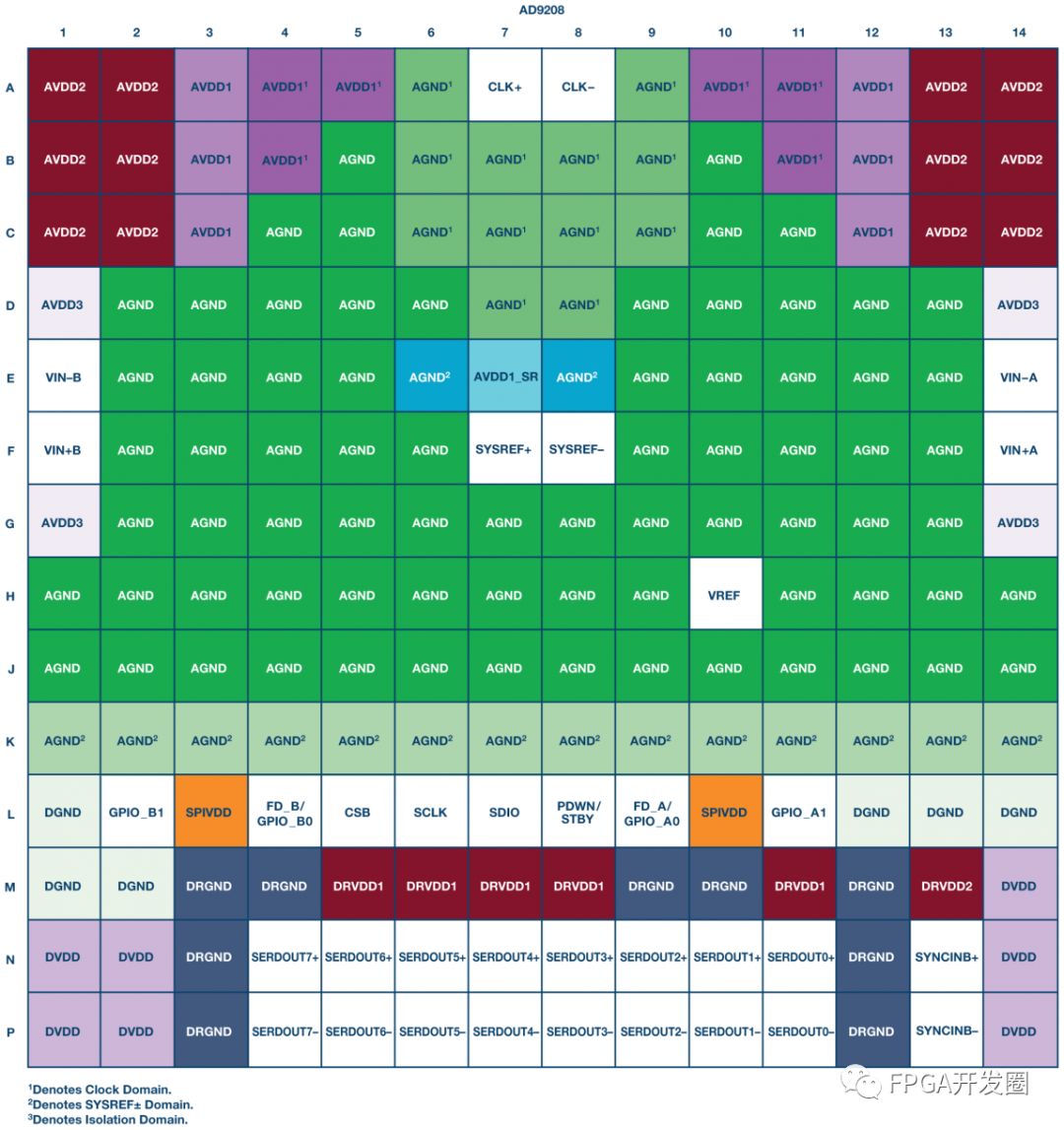
As the industry shifts to deep sub-micron technology and high-speed switching circuits, the level of functional integration is increasing. Take AD9467 and AD9208 as examples, AD9467 adopts 180 nm BiCMOS craft, and AD9208 adopts 28 nm CMOS craft. Of course, the noise density of AD9467 is about -157 dBF S/Hz, while the noise density of AD9208 is about -152 dBF S/Hz. However, if you take the data sheet and do a simple calculation, take the total power consumption (per channel) and divide it by the resolution and sampling rate, you can see that the power consumption of AD9467 is about 330μW/bit/MSPS, while AD9208 Only 40μW/bit/MSPS. Compared with AD9467, AD9208 has higher sampling rate (3 GSPS to 250 MSPS) and much higher input bandwidth (9 GHz to 0.9 GHz), and integrates more digital features. A D9208 can complete all these tasks, and the power consumption per MSPS is only about 1/8. The power consumption per bit per MSPS is not an industry standard indicator. Its role in this example is to highlight the benefits of using a smaller size process in ADC design. When ultra-fast circuits operate at very close distances, there is always a risk of coupling or tremor between modules. To improve isolation, designers must consider various coupling mechanisms. The most obvious mechanism is through shared power domains. If the power domain is as far away as possible from the circuit, the possibility of chattering in digital and analog circuits that share the same voltage rail (0.975 V for AD9208) will be very small. In silicon, the power source has been separated, as is the ground. The package design continues to implement this isolated power domain processing. The resulting division of different power domains and grounds in the same package is shown in Table 2, which takes AD9208 as an example.
Show the pin arrangement diagram of each different domain of AD9208.

Figure 1. AD9208 pin configuration (top view)
This may panic the system designer. At first glance, the data sheet gives the impression that these fields need to be handled separately to optimize system performance.
Can't see the end?
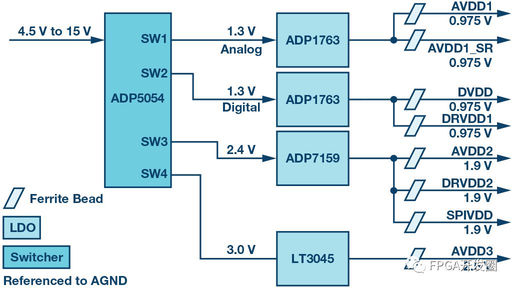
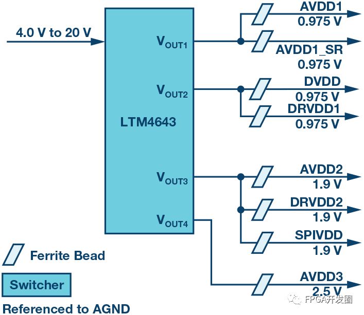
The situation is not as terrible as it seems. The purpose of the data manual is only to arouse people's attention to various sensitive domains, so that system designers can pay attention to the PDN (power delivery network) design and divide it appropriately. Most power domains and ground domains that share the same power rail can be combined, so PDN can be simplified. This leads to a simplified BOM (bill of materials) and layout. According to design constraints, Figure 2 and Figure 3 show two PDN design methods for AD9208.

Figure 2. AD9208 pin configuration (top view)

Figure 3. AD9208 PDN, DC-DC converter powers all domains
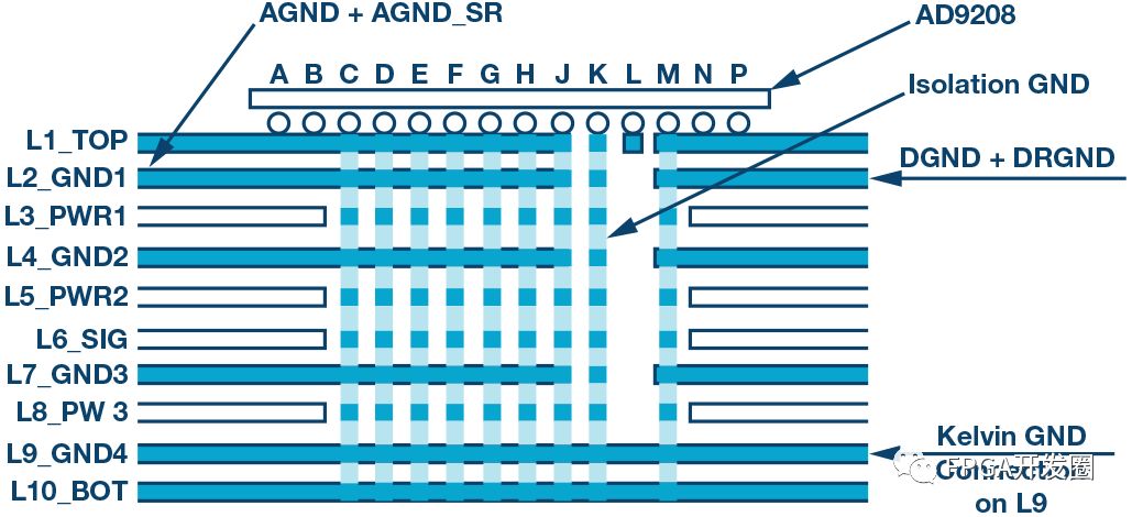
Through sufficient filtering and layout separation, each domain can be rationally arranged to maximize ADC performance while reducing BOM and PDN complexity. The Kelvin connection method for each ground domain will also improve isolation. From a netlist perspective, there is still only one GND net. The circuit board can be divided into different ground domains to provide sufficient isolation. In the AD9208-3000EBZ, the evaluation board of the AD9208, different ground zones form a Kelvin connection on the 9th layer. Figure 4 shows a cross section of the 10-layer PCB (printed circuit board) AD9208-3000EBZ, which shows the different GND connections.

Figure 4. AD9208-3000 EBZ PCB cross section under AD9208
So, this is not the end of the world?
Absolutely not. Just because the AD9208 data sheet shows all these fields, it does not mean that they must all be separated on the system board. Understanding the system performance target and ADC target performance plays an important role in optimizing the PDN of the ADC. The use of smart partitioning on the circuit board to reduce unnecessary ground loops is the key to minimize crosstalk between domains. Sharing power domains appropriately while meeting isolation requirements will simplify PDN and BOM.
SMC Cable Mount Connectors,SMC Bulkhead Mount Connectors,SMC Flange Mount Connectors,SMC PCB Mount Connectors
Xi'an KNT Scien-tech Co., Ltd , https://www.honorconnector.com