This design example analyzes several flawed circuit designs, including a Class D switching audio power amplifier causing a severe "engineering disaster." This amateur class D amplifier design has neither negative feedback nor output filtering and was published in the most popular electronic enthusiast magazine in the United States. Due to the necessity of the external connection of the input and output of the amplifier circuit itself, lack of isolation measures may cause serious safety problems.
As far as the publishing channels of electronic design articles are concerned, they can be divided into two basic categories: professional and personal hobby. In general, it is possible to determine what content is available for publication and what content cannot be published. The personal hobbies used to have magazines such as Popular Electronics and Electronics World. These magazines are available in supermarkets. Their main target readers are individual lovers. EDN and Electronic Design (ED) are the best representatives of professional magazines.
In general, almost any circuit design can be safely published on EDN and ED because professional readers usually understand any obvious dangers, and professional authors will generally explain in detail most dangerous circuits. But magazines for enthusiasts should (I say it should, because they often ignore this requirement) adhere to certain standards and avoid publishing dangerous circuit designs. Although society and the legal system have increasingly stringent requirements for the issuance of dangers, the dangerous circuit design continues to be published in the last few years before the publication of these personal enthusiast magazines.
Apart from hazards, there are good and bad circuit designs. A circuit may be a good design or it may be garbage. Regardless of professional or enthusiast magazines, there are a certain number of inferior circuit designs. Perhaps you think professionals in the publishing industry should play a role in quality control to some extent to ensure that only high-quality circuit designs can be published. However, the problem is that many really good engineers are busy designing in the company. This is just like many other industries.
Getting involved in dangerous areasLet us look at one of the most memorable electrical engineering design disasters. What struck me was that it was released in the most popular electronic enthusiast magazine in 1996 and it was irresponsible to publish this circuit design. In addition, there are some less serious but still important issues.
This circuit is used for Class-D switching audio power amplifiers. This technology was introduced not only as far back as 1975 (in these very popular electronic enthusiast magazines), but also during this period. The first commercial switching audio power amplifier. At the time, Sony developed a V-FET device named after the vertical J-FET type structure. As FETs, these devices easily achieve the high-speed requirements of a 250kHz switching frequency matched to high-quality audio (this means that the sampling rate is an order of magnitude higher than the ideal upper frequency). The basic topology of a generalized Class D amplifier is similar to that of a Sigma-Delta modulator:
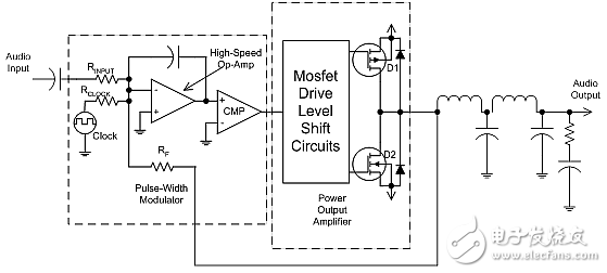
Figure 1: The basic topology of a properly designed Class D switch audio power amplifier.
It should be noted that the design of this generalized topology is correct. The modulator is contained within a closed feedback loop to ensure faithful restoration of the input signal. The output filter is external to the feedback loop, greatly simplifying the stability problem and actually supporting more bandwidth. This basic topology diagram omits many details. For example, the gate drivers of power devices (including Sony's original V-FETs) pose some challenges for circuits such as cascade followers.
One of the difficulties unique to Class D switch designs is that they rely on the recycling of unused energy in the output stage to achieve its efficiency. Problems arise when a DC voltage drive is provided to the load from a single output stage. We can use the basic circuit in Figure 2 to explain. The circuit shown in Figure 2 is based on the assumption that we are trying to generate a negative output voltage. It also includes devices that do not appear in real circuits, like D3 and D4. The purpose of adding these two diodes is to emphasize the fact that most power supplies have good current-carrying characteristics, but the current is very poor.
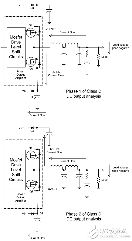
Figure 2: This circuit shows that single-ended Class D can only be used for AC signals without DC components.
The circuit shown in Figure 2 above illustrates that the lower MOSFET Q2 turns on, supplying the load with the necessary current to produce a negative output. Any intermediate output voltage determines a duty cycle of less than 100% (or more than 0%), so as shown in the bottom diagram, Q2 turns off and Q1 turns on. Under these conditions, due to the effect of the inductor in the output filter, the current continues to flow in the same direction. The only channel is from the Q2 source, through the D1 flyback diode, to the Q2 drain, and then into the positive supply. Such a direction of current causes the positive supply voltage to rise a little at each cycle until it is high enough to damage the circuit device.
This circuit cannot be exposed at the DC input, nor can it form an offset that can appear as a static DC output. In this case, the output energy of the output filter will increase the supply voltage on the rail opposite to the load supply (for example, the positive DC level of the load will act as a boost to the negative rail). Sony handles this problem with AC-coupled inputs, built-in a "voltage rise detector" that turns off the amplifier. A more clever solution is to set up the switching amplifier as a full bridge so that energy can be recovered.
A serious engineering design disasterNow that we have outlined the basics of a well-designed class D amplifier, let's take a look at the so-called “engineering disaster†through two schematics (the amplifier in Figure 3 and the power supply design in Figure 4). ". Obviously, this amateur class D amplifier design has neither negative feedback nor output filtering. This is an open-loop architecture with a switching frequency of 50 kHz. Yes, it is feasible, but it is definitely not up to the level of high fidelity.
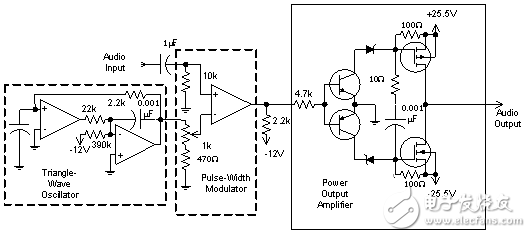
Figure 3: This is the simplest implementation of a pulse width modulator. It is an open loop and there is no output filter. This is a very rough design.
The amplifier can work without output filtering, after all, the speaker cannot respond to 50kHz. Filtering can improve the serious distortion problems that this circuit can produce. Worse consequences are RFI (radio frequency interference) problems from longer speaker leads, which carry 50kHz switching waveforms with a large number of powerful harmonics. This is likely to bother your neighbors.
The pulse width modulator consists of the most basic comparators. One side of the PWM is a triangular waveform and the other side is the desired analog signal. Given the low switching frequency of 50 kHz, the circuit that couples the comparator output to the power device can only be as simple as possible.
There is no current limit or other protection for the output device. Short-circuiting the speaker leads will certainly lead to catastrophic consequences. Not to mention other risks that may arise, such as short circuit and high current output devices may cause fire.
If this is not a circuit that is awkward and hardly worth the expense of money or time to design, then this design is the largest disaster non-power design. Please note that the author started with old-fashioned tube equipment, such as a 5-tube transformerless radio design whose internal circuitry is directly connected to the AC end. However, at that time, the manufacturer was also very good in this respect. You will not see any type of external connector hole, and any customer may touch or grasp it with careful insulation. Therefore, I am no stranger to the operation of the equipment directly connected to the AC power supply. It can handle it well, but it is easily overlooked.
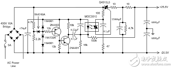
Figure 4: Do not design such a power supply circuit. If you must do this, it must be connected to AC power through an isolation transformer.
Again, the power of this amplifier directly connected to the AC is just a basic problem. Due to the necessity of the external connection of the input and output of the amplifier circuit itself, lack of isolation measures may cause more dangerous consequences. When AC power is on, the user may be exposed to the cable.
Some readers may observe that there are no obvious "direct" connections on either side of the AC wires in the diagram, such as input jacks or speaker connections. Let me explain this. When you use the AC power cord, you will face one of the following two scenarios: 1) No insulation; 2) Insulation (Use some kind of transformer to completely isolate the AC line). In scenario 2, it is absolutely impossible to generate current through the AC line through any connection on the amplifier, and thus absolutely ensure the electrical safety of the operator. The amplifiers described here do not have this isolation. Although the current path of the AC line can be established via rectifiers, filter caps, TRIACs, and some resistors, it is still extremely risky once it reaches out to people. The AC power cord is the most dangerous source of electrical energy that we usually come into contact with. When people are exposed to AC connections, insulation is absolutely necessary. This is undoubtedly true.
This extends to AC line security issues, including the polarity of the AC power line, ensuring that the low end is always on the same side as the ground. However, all these problems should be avoided in any well-designed circuit, and the measures taken are to use a power transformer. The amplifiers discussed earlier simply need to include a commonly used isolation transformer to ensure safety (but not necessarily good).
As a follower, it is worth mentioning that the magazine issued some statements in subsequent journals, pointing out that this circuit design lacks isolation. However, for beginners, it is really terrible to try such a design from the beginning.
In addition to the above issues, this power supply design is ingenious in some ways. It uses TRIAC AC line phase control as an efficient "coarse" regulator for 51V power supplies. However, when you understand that phase-controlled tuning produces a fairly large RFI, and it is contrary to modern power supply design, it is less clever. Modern power supply design focuses on power factor correction, introduces the waveform and phase of the current waveform diagram, and makes it as consistent as possible with the voltage waveform diagram (see Phase Control Dimmer). In short, the current in the power supply flows along the voltage waveform of the alternating current sine wave, flowing in multiple short bursts. The spectrum will look very messy. Obviously, this is only one of the smaller issues.
Problem of disqualificationIn the 1980s, a magazine sponsored by a prominent government research institute published a design note on how to achieve higher bandwidth through operational amplifier circuits. It contains only a simple, very general schematic (Figure 5).

Figure 5: This circuit is considered a viable way to increase the bandwidth of the op amp circuit. In fact, this may be one of the most unstable structures of the op amp.
Anyone who has a basic understanding of operational amplifiers and feedback theory will easily realize that assuming that the op amp's open-loop gain is significantly higher than the feedback resistor ratio, the signal gain can only be set by the ratio of the feedback resistor. When the open-loop gain falls to be equal to or less than the value set based on the feedback resistance, the frequency at this time determines the bandwidth. Unless you select a different op amp, you cannot improve the gain-to-frequency relationship of the open-loop gain.
Simple tests show that we are placing a pole in the feedback path of the monopole system. This situation will only make the system more unstable.
The only possible effect of this type of capacitance is the increased transient response overshoot, and a significant increase in high-frequency noise (possibly the authors have noticed an increase in high-frequency noise and thus inferred higher bandwidth). In some cases, direct oscillations also occur.
fake-scienceAround mid-1996, an electronic enthusiast magazine published an article on magic lights, claiming that by simply applying a common desk lamp dimmer circuit, the efficiency of incandescent lamps can be greatly improved. In fact, this circuit is even worse because it is a half wave.
The authors claim that using a 30V light bulb instead of a 100V light bulb has only one-third the voltage and current, which saves 90% of the electrical energy.
Someone immediately began to wonder, such as how to compare the light output (use photometer measurement is obvious, but it is easy to have measurement error), and pointed out that the 30V light bulb is no lower than the 110V bulb temperature. However, the key mistake here is that in the 126o delayed half-wave phase control, there is a huge 3:1 difference between the mean and the rms rms.
This design is popular because the author uses a very basic, inexpensive instrument to measure voltage and current, and it measures nonlinear waveforms. More surprisingly, this design method was also granted a patent (U.S. Patent 5,463,307).
To try to understand the measurement method for this type of circuit, the author performed some measurements on the full-wave TRIAC dimmer circuit, as shown in Figure 6. The difference between this circuit and the magic lamp circuit is that the magic lamp is half wave, and this circuit is full wave, but it can explain the problem in measurement.
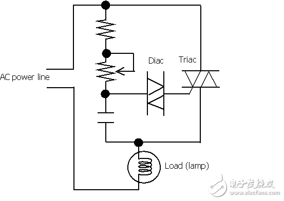
Figure 6: TRIAC dimmer circuit.
As the AC voltage across the dimmer increases at each cycle, the capacitor begins to charge. When about 30V is reached, the DIAC will break and conduct, dropping the voltage low enough to allow the capacitor to discharge, triggering the TRIAC. Since this is an AC semiconductor, it is repeated every half cycle.
In Figure 7, we can see a photo with an oscilloscope inside to measure the voltage across the load of the desk lamp and an average average AC voltmeter in parallel. The oscilloscope measurement function is set to measure the period rms voltage. Figure 7 shows the result of the current measurement (via a 2 Ω resistor). If you use this meter to calculate power, you can conclude that the load consumes 33mA at 32.7V and consumes 1.08W. In fact, it consumes 56mA at 55V and consumes 3.08W.
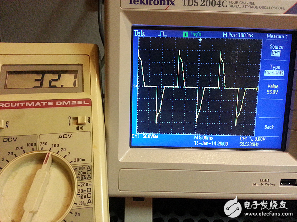
Figure 7: The oscilloscope is set up to measure the load voltage and a traditional average AC meter is connected in parallel. Note that the actual effective value that the oscilloscope measurement function can capture is 55V, while the meter shows 32V.
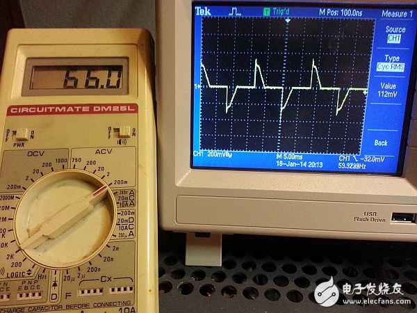
Figure 8: The setup in Figure 7 is to measure the current through a 2Ω resistor. Again, the average measurement is inaccurate and its readings are low.
UPS-Charged Pure Sine Wave Inverter
Saintish inverter charger power ranges from 500W to 4000W. and DC voltage available in 12V, 24V or 48V.
It works as like UPS, when the public main power is available, the Inverter with charger will charge battery, when the main power disconnected, the inverter stop charging the battery immediately and transfer power from DC to AC, supplying the loads. All goes so fast the loads keep working without any problem.
Ups-Charged Pure Sine Wave Inverter, Inverter With Charger, Inverter Charger 2000W
Hangzhou Saintish Technology Co.,Ltd. , https://www.saintishtech.com