Regarding the measurement of the PN junction temperature, the thermal resistance method is generally used to measure the junction temperature at the application end of the semiconductor device. However, this method has limitations for the LED device and has been erroneously applied in many cases. The mistakes and limitations of applying the thermal resistance method have been elaborated in [1]. I think we should abandon the thermal resistance method.
There are many new ways to measure the junction temperature, but some of these methods may not reflect the junction temperature well. Infrared imaging, for example, theoretically measures the temperature of the device surface or the surface of the chip, and it is impossible to measure the temperature at the actual PN junction. The spectroscopic method is only available for individual professional testing organizations. The instrument is expensive and not suitable for the daily work of device users.
In fact, whether it is from professional measurement or amateur measurement, the simplest, most accurate, and most basic, or voltage method is to measure the junction temperature. The thermal resistance method is actually derived from the voltage method. Due to the low cost of measuring instruments with a measurement accuracy of 1mV, there is no need for the device user to use a thermal resistance method to measure the junction temperature.
This article mainly introduces the voltage method to measure the junction temperature. The thermal resistance method was also used to measure the junction temperature, and the problem of thermal resistance was proposed. Finally, some other methods for measuring the junction temperature are briefly described.
The voltage method for calculating the junction temperature introduced in this paper is from the perspective of general engineering application. Mainly for the general device manufacturers and device users to provide their own testing methods. Therefore, some of the instruments used cannot be compared with professional instruments, but there is no need to worry about accuracy and accuracy. In this regard, as long as you understand the principles of physics, you will understand. The key is to look at the specific operator's design of the testing organization and the choice of instruments, and the meticulous degree of operation.
Although this article is mainly focused on LEDs, it can also be extended to the junction temperature measurement of other semiconductor devices. Because the PN junction of the LED and the PN junction of other semiconductor devices are in principle the same.
Chapter 1 Voltage Measurement of Junction Temperature
Section 1 Theoretical Basis for Measuring the Junction Temperature by Voltage Method
According to semiconductor physics theory, the forward voltage, current, and PN junction temperature of an ideal PN junction have the following relationship [2]:

-(1)
In the formula:
U: PN junction voltage; I: current;
T: junction temperature; k: Boltzmann constant
C: parameters related to chip manufacturing;
Eg: Bandgap Width; q: Electronic Battery
From equation (1), it can be seen that for a finished device, voltage is related to temperature and is linear. In addition to current parameters, some other parameters are constants. Therefore, when a certain current value is fixed (ie, the current is also a constant), the voltage is only linearly related to the temperature.
From this, we can calculate the junction temperature by measuring the voltage. And the physical calculation of formula (1) can be converted into pure mathematical calculation. That is, the numerical relationship between voltage and junction temperature can be expressed by a linear equation. As long as the slope of this straight line is obtained, the junction temperature at this thermally stable temperature can be obtained by measuring the voltage at a known junction temperature and the voltage in the thermal steady state.
In the Cartesian Cartesian coordinate system, temperature is the abscissa (independent variable) and voltage is the ordinate (function). According to the linear equation, the slope of the line is calculated as:

In the formula:
Us - forward voltage at higher junction temperature Tj
Ua - forward voltage at lower junction temperature Ta
K - PN junction voltage temperature coefficient (straight slope)
In this way, the higher junction temperature Tj can be calculated using the following formula:

Formula (3) is the basis used by us to measure the junction temperature. In practical applications where the junction temperature is measured, Ta is often ambient temperature, and Tj is the junction temperature at thermal steady state.
According to equation (3), to measure the junction temperature, it is necessary to first know the voltage temperature coefficient K of the PN junction. The second section will describe how to measure the K-factor and related problems.
From equation (1), we can see that there are three variables in the formula for the finished device: voltage, current, and temperature. In formula (2), we set a precondition that the current is a fixed value. It seems that the K factor is related to the current value. However, tests on actual products have found that the K-factor values ​​or curves at different currents are the same. This is a key issue. It is with such a result that we can easily calculate the junction temperature. The phenomenon that the K factor is independent of the current will be explained in Section II.
Note that this is the measured junction temperature, not the junction temperature. Because the junction temperature cannot be directly measured with a temperature measurement device, it can only be calculated after some relevant parameters are measured.
Section 2 Measurement of K Coefficients
1. Principle of measuring K-factor
According to the linear relationship between voltage and temperature, at a certain current value, as long as the voltage corresponding to the PN junction at any two temperature points is tested, the slope K value can be calculated according to formula (2). This is the basic principle of measuring and calculating the K-factor.
2. Description of the K factor
Although theoretically the voltage and temperature of the PN junction are linear, that is the ideal theoretical PN junction. The actual situation is not the case! The actual measured voltage-temperature relationship of the LED device is not necessarily a good linearity. This is not caused by a test error because testing the same device at different times results in the same result. According to my test results for some LEDs, the report in [3] and OSRAM's product specification, the voltage temperature coefficient of LEDs is not always a good linear relationship. This depends on the specific product. I tested voltage temperature coefficients for several different packages and different power LEDs. See Figure 1.
In Figure 1, the black points represent measured data points, the black curves are fitting curves, and the red dotted lines are end-to-end reference lines. It can be seen that most of the K-curves are curved downwards by some meniscus shapes, with inflection points approximately between 70 and 80 degrees. Before and after the inflection point can be approximated as a straight line. The difference between the slopes of these two approximate lines is often still very obvious. Of course, there are some LED K curves that are almost linear. The top two K lines in Figure 1.
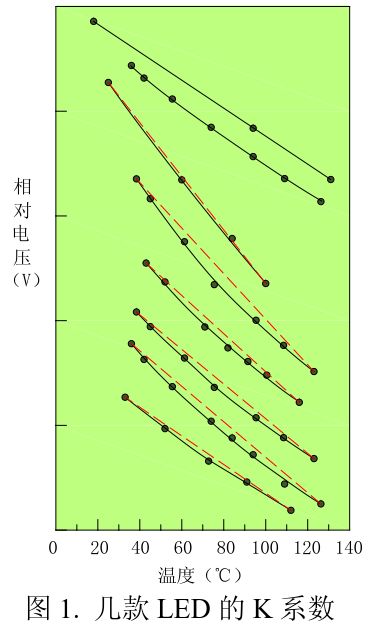
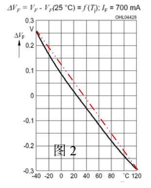
Figure 2 shows the voltage and temperature profile of an OSRAM 3535 packaged LED. As you can see, it is not a very good straight line. It is also a downward curve. The red dotted line in the figure is the reference line added by others. Similarly, on this curve, in the range of 20°C to 120°C, 80°C can also be used as the boundary to obtain two straight lines with good fit.
The phenomenon that the curve of the K-factor curve is bent as the temperature rises and the voltage decrease trend becomes gentle is discussed in [3] and [4]. My opinion is: Since the PN junction cannot completely disappear within a reasonable external voltage range (the so-called reasonable applied voltage range means that the applied voltage should not be too high and the device burns), but the applied forward voltage exceeds When a certain value or temperature rises, the speed at which the barrier region narrows becomes slower, that is, the junction voltage declines gradually; the internal resistance increases as the temperature increases and the voltage increases, and the two become destructive. The tendency of VF to decrease with increasing temperature becomes slower. The influence of the resistance of the package body and the resistance of the electrode on the chip, etc., is less affected at lower temperatures. When the temperature is higher than a certain value, the influence of these resistances increases, which results in a slower voltage decrease. For more than 70 ~ 80 °C curve becomes slow, not only with the parasitic resistance, but also with the chip size, packaging structure and other factors.
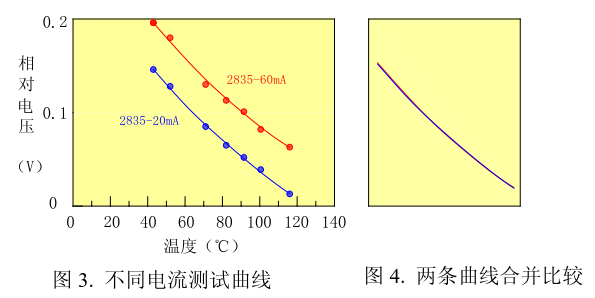
For example, a white LED of type 2835 with a current rating of 60mA has basically the same results at 20mA and 60mA tests, and is not affected by the size of the current. That is, the parasitic resistance is not affected by the heat generated by the current. See Figure 7. It can be seen that the factors that cause the curve to curve are various.
Since the actual K factor is generally not a good straight line but a curve, it is recommended to provide a K-factor curve. Compared to providing only a specific K value, the error can be reduced. A single K value may bring about a large error without using meaning. Although two K values ​​can be approximated as straight lines before and after the inflection point, there are difficulties in practical application. In this regard, ask the reader to think for himself. It is not recommended to do this.
3. Effect of test current size on K-factor
In many literatures and standards, it is recommended to use very small currents when testing K values ​​in order to reduce the effect of heat generated by the current. Large currents, of course, generate heat. However, with each test, because of the very short time, the same current causes the same temperature rise. That is, the current causes additional voltage and the same amount of temperature change. Because what we need is two-point data relative value, not absolute value. When calculating the slope of the line, the additional voltage and temperature variation can be completely eliminated by subtracting the two voltage values ​​and temperature values. Similarly, the inherent error of the test instrument itself will be eliminated by subtracting it.
Figure 3 shows the K-factor curve of a Model 2835 LED (rated at 60mA) at various currents. The points in the figure are measured data and the curves are fitting curves. Figure 4 shows the situation where the two curves are overlapped. You can see that they basically coincide.
Looking at the curve of the OSRAM test (see Figure 2), you can see that the test current is 700mA. He also did not use a small current to test.
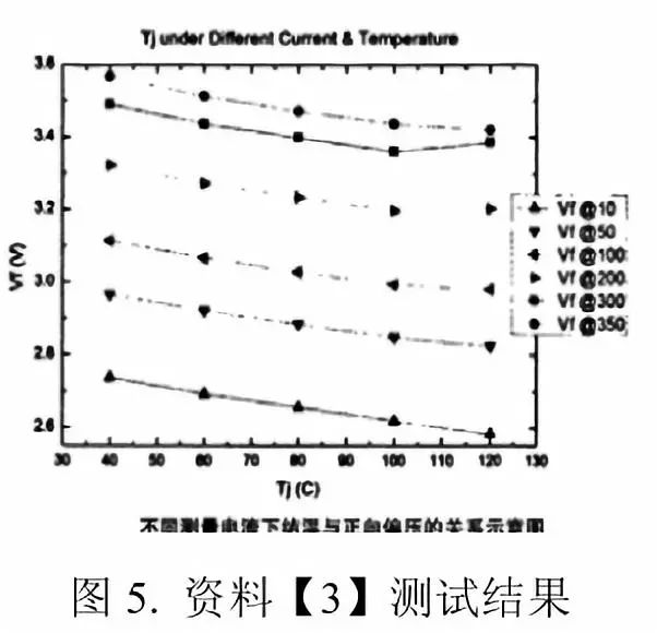
Figure 5 is the test result of [3]. The K-factors of different voltage current curves measured under different currents (from 10mA to 350mA) are basically the same under 100°C. (The reader can use some graphics software to intercept a curve.) Moving to other curves, you can see that they are basically coincident).
As for the problems occurring above 100°C, I hereby make the following inferences based on the contents of [3]:
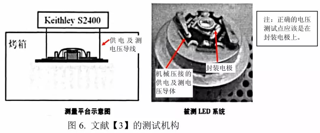
According to the test method of reference [3], referring to FIG. 6, the contact between the conductor of the power supply and the voltage to be measured and the LED during the test is mechanical crimping, which easily generates a contact resistance, and the contact resistance may produce a relatively large temperature change. Big deviation. In addition, the voltage test point is far from the electrode of the LED package, and the power supply and the voltage measurement are the same. This does not meet the requirement of the four-wire method, and the resistance outside the package will introduce errors. As can be seen from Figure 5, not every current at a higher temperature results in a large increase in voltage. At 300mA, the voltage tested at 120°C is significantly more severe than at other currents, and the voltage increase is not high at 350mA. I have done experiments and heated the LED to 300°C and still found that the voltage is monotonically decreasing. Therefore, I inferred that the voltage increase in the literature [3] at higher temperatures may be related to the parasitic resistance introduced by its test mechanism.
As a result of my own test, when the temperature was as high as 120°C, there was no abnormal voltage rise described in [3]. See Figure 1.
From the above example, it can be seen that the test current size has almost no effect on the shape of the K-factor plot. The only effect is the position on the ordinate of the K-factor curve at different currents. Or, the graph of K factor shifts up and down as the current changes.
It is important that the test current has no influence on the K-factor curve. This is very beneficial to the practical application of the K factor to measure the junction temperature. Because, the K-factor value or curve measured at any current can be directly applied to the actual arbitrary current working state to measure the junction temperature. In this way, the junction temperature under the actual working condition of the test device can directly measure the voltage of the relevant temperature point, and it is not necessary to measure the voltage by reducing the current to the small current when measuring the K value. Under actual working conditions, such as an off-the-shelf luminaire, the original power supply is not capable of instantaneously reducing the current to the current level at which K is measured. Therefore, the methods used to measure the junction temperature by using the K factor introduced in the prior literature are not practical and have errors because of changing the current measurement voltage. From the content described in this article, there is absolutely no need to do so.
4. K coefficient measurement method
(1) Test Precautions
To measure the voltage temperature coefficient of a semiconductor device, a four-wire method should be adopted, ie, two lines are used to power the LED, and two other lines are used to access a high-precision digital voltmeter. The line connecting the voltmeter should be as close as possible to the device package electrode. The purpose of this is to minimize the effect of the voltage drop across the current on the resistance of the PN junction. In particular, when the temperature variation range is large, the resistivity of the wire is often a function of the temperature. In this way, the same wire, with different resistance at different temperatures, introduces voltage errors. At the same time, the voltage measuring wire should use thinner wires to avoid influence of the heat conduction of the wire on the device temperature. At the same time, it should be noted that the wire for measuring the voltage must be welded, instead of mechanical crimping to avoid the influence of the contact resistance. When mechanical crimping is used, due to factors such as the unevenness of the contact surface, the contact resistance increases due to deformation at a higher temperature, so that the measured voltage deviation is usually manifested as high voltage, that is, abnormal upward curling of the high-temperature curve.
According to experience, the voltage temperature coefficient of LED is generally between -1.4 and -2.6mV/°C. For engineering applications, the voltmeter display accuracy should reach the millivolt level. For a 4-digit half-digital multimeter, in the 20V range, measuring 10V or less can be displayed to 1mV, so the error is 0.5mV (such as 3.0005V for 3.0005V display and 3.000V for 3.0002V display). (In this way, even with an error of 0.5mV, the maximum temperature error for a K value of -1.4mV/°C is approximately 0.4°C.) Of course, it is better to have a higher-precision voltmeter.
Occasional errors may occur at some test points in the test. Therefore, it is recommended that some temperature points should be tested during the test. Generally in the range of 20 to 140 degrees (under the amateur condition, it may be inconvenient to make a low-temperature environment, the low-end temperature may be selected as 30 to 40 DEG C), and one test point is selected every 20 degrees. In actual testing, the temperature value does not have to reach an integer value and a very precise interval. Because the actual use of the calculated junction temperature does not require these actually tested values ​​to obtain the K value or curve, the data of these tests are processed. The data processing method will be described below.
This article is not about researching and manufacturing specialized and commercialized test instruments. Therefore, the testing organization introduced seems relatively crude to a professional instrument. However, if you understand the principle of testing, the simple organization can also guarantee the test requirements. The so-called "simply" means that the testing organization that you build yourself does not need to have any beautiful appearance of the instrument, or how it is structured. The purpose of this paper is to allow general device manufacturers and device users to use their own conditions to test K-factors and measure the junction temperature of devices in actual use.
(2) Method for specific testing of K factor
1 Prepare a thermostatic device that can use a commercial incubator. If not, a heating platform with a better temperature control device can be used and then a housing can be used to cover the device, thus forming a simple thermostatic chamber. Note that the shell is preferably made of thicker material with poor thermal conductivity, and the cavity should be as large as possible in order to avoid the influence of the outside temperature as much as possible, and to ensure that the inside of the chamber can maintain a constant temperature. See Figure 7.
2 Solder the positive and negative electrodes of the device with two leads, one for the device and the other for the voltmeter. Then place the device in a constant temperature room. (In particular, care should be taken to use thinner wires for low power or small devices.) Referring to Figure 8, the red and blue wires are used to connect the power supply, and the orange and green wires are used to connect to the voltmeter.
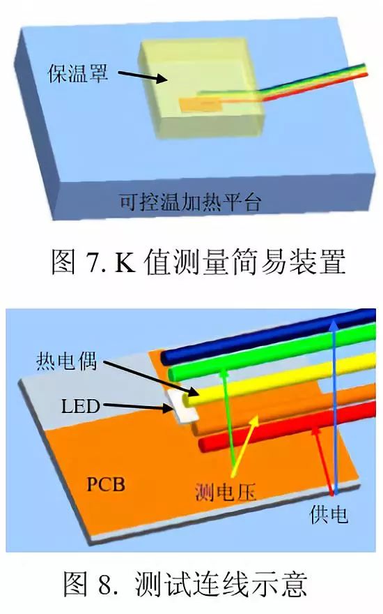
3 Fix a thermocouple on the device to measure the temperature of the device. When heated to a certain temperature and constant temperature, the temperature of the PN junction is also this temperature. The accuracy of the thermometer must reach 0.1 °C. Referring to Figure 8, the yellow line represents a thermocouple.
Note that the temperature probe is as far away from the heating platform as possible. Contact with the LED light emitting surface, or contact with the electrode closest to the LED heat sink or PCB copper foil.
4 Start the heating platform to start heating and set a constant temperature.
Note that the set temperature of the heating platform is not the temperature on the device. The temperature of the device should be based on the temperature of the temperature probe set on the device in the holding chamber.
5 After reaching a constant temperature at a certain test temperature point (typically the temperature does not change by more than 0.5°C within 15 minutes), the device is powered in a constant current mode and the initial instantaneous maximum value of the device terminal voltage is measured. Then stop the power supply and start heating up to the next temperature point before testing.
Tip: Since the voltage on the device is established and the instrument responds to the measured signal for a certain period of time, and this time is relatively short, the voltage display initially appears to rise and starts to fall in a very short period of time. The maximum value must be read. It is often not easy and it is easy to miss readings. It is recommended to use the camera to record the meter display so that when the reading is missed, you can look back at the recording to obtain the maximum voltage.
Record the corresponding voltage value at each test temperature. Note that if one read voltage is unsuccessful, stop the power supply for a long enough time to return the PN junction temperature to a constant temperature and then retest. Do not operate continuously.
5. Data processing
The data after the test is completed is processed and analyzed. Fit the data into a smooth plot. When fitting the curve, it should be noted that the measured data should be evenly distributed on both sides of the fitted curve (additional data with large deviations should also be excluded). Note that do not use AutoCAD software to automatically generate spline curves based on point coordinates.
For a fitted curve, don't change it to a straight line because it looks like it is straight. This can lead to great errors. However, for some LED's K-factor characteristics, the error can be considered based on the calculation. If the error is within 3°C in the range of the junction temperature between 0°C and 140°C, it can be processed with a straight line.
The measured K-factor curve will actually be a typical feature of a model specification product and it does not represent the actual parameters of a specific product in that product. Because the curve can be considered the same for the same specification product, the specific VF value of each product is different. If you measure the K curve for each product, you will see that the curves have the same shape, but the position in the coordinate system is different. That is, the voltages of different samples at the same junction temperature may be different.
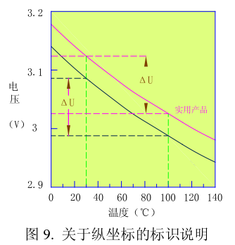
For example, as shown in Figure 9, the potential K curve and test sample of a practical product are the same, but the VF of the two is different. For example, when the ambient temperature is 30°C, the voltage value of the practical product is tested, and the voltage of the test sample at this temperature is different. When the junction temperature is constant at a certain temperature (eg, 100° C.), the voltages of the two are still different. However, the voltage difference between the two at any two temperatures is the same.
Therefore, the ordinate of the K-factor curve given in the specification is not meaningfully identified by the VF value of the actual sample. Because in the real application, this curve of "utility product" in Fig. 9 does not exist in the specification book, but only the curve of the test sample. We use the curve of the test sample to calculate the junction temperature.
Therefore, the ordinate is preferably identified using "relative voltage" or "reference voltage." "Relative voltage" means that the value indicated on the y-coordinate indicates the relative value of the voltage between points on the curve. Using the concept of "relative voltage", the two curves in Figure 9 can actually be combined into a single curve. FIG. 9 can be represented as FIG. Note the numerical difference between the ordinates in Figure 9 and Figure 10.
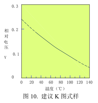
Of course, for the way of “relative voltage†identification value, it is not necessary to use only the conversion method shown in Fig. 9 to Fig. 10, that is, the original measured data 2.9V is redefined as 0V point. The voltage value corresponding to 25°C (you can also use any temperature point) can also be defined as the vertical axis 0V point similar to Figure 2. However, this will cause negative values ​​on the ordinate.
The determination of the 0V point on the vertical axis is not mandatory or standard.
For the part of the measured upper and lower temperatures, it can be extended outward according to the trend of the curve. For example, the minimum temperature selected during the actual measurement is 30°C, and the maximum temperature is 100°C. For parts less than 30°C and greater than 100°C, the trend extends outward according to the trend of the curve. Extensions can be expressed in dotted lines. As shown in Figure 10, the dashed line is not measured, but extends outward according to the trend of the solid line.
When making k-line graphs, coordinate scales should be subdivided as much as possible to facilitate the user's calculation. Especially on the ordinate, since the voltage change is measured in millivolts, the ordinate should be expanded as much as possible to make the graph appear steeper to reduce the measurement coordinate reading error.
6. Recommendations on Device Manufacturers Providing K Values
It is recommended that manufacturers of semiconductor devices should provide the user with a voltage-temperature curve of the device in the specification, rather than a single K value.
7. K coefficient measurement error
The K-factor measurement error mainly comes from two aspects: one is the resistance of the device structure material; the second is the resistance introduced by the test structure; and the third is the factor of the test device. Let's talk about them separately.
(1) Effect of device structure material resistance
The resistance components of the device itself are mainly: the resistance of the P-type region, the N-type region, and the PN junction region; the resistance of the electrode material on the device, the resistance of the die bonding material (for the chip of the vertical conductive structure), and the chip-to-stand Metal lead resistance, bracket body resistance.
The P region, N region, and PN junction resistance of semiconductor materials are negative temperature coefficients. This is the main body of our investigation. The resistance of the package material is a positive temperature coefficient, which is the resistor we don't want. When the temperature changes, the voltage changes caused by these two types of resistance cancel each other out. Therefore, the parasitic resistance of the internal package material is one of the sources of error.
In general, the resistance of the electrode material is already considered in the design of the chip itself, and it is designed to minimize it as much as possible. However, larger parasitic resistance may be introduced during chip packaging. For example, the chip-to-package electrode wire solder joints have poor soldering, and the vertical conductive chip adhesive sheet silver paste resistance. Of course, under normal good packaging process, this parasitic resistance will usually be very small. When we discuss the K-factor measurement problem, it is premised on a good packaging process.
From our actual testing and experience of LEDs, we can see that the LED's voltage will always fall when the temperature rises within the allowable operating temperature range of the LED chip. This shows that the variation of the resistance of the semiconductor material with temperature is the main one, and the resistance effect of the packaging material is secondary. Usually the resistance of the packaging material is very small, even if it changes with increasing temperature, its variables are often negligible. In this way, when we test the K-factor, we can ignore the part of the package body resistance that changes with temperature, that is, it is considered that it does not change with temperature. When calculating the K factor, the voltage on the package body resistance can be eliminated by subtraction calculation (according to the principle of formula 2).
(2) Effect of test structure resistance
The resistance of the test mechanism is usually a positive temperature coefficient, and the resistance value varies at different temperatures. Therefore, the resistance introduced by the test institute is required to be as small as possible. Therefore, when the K factor is required to be tested, the end point of the voltage measurement should be as close to the electrode of the package as possible to avoid the error introduced by the resistance other than the electrode with the temperature change. And it is required that the power supply wire and the voltage measuring wire should have good welding, and the crimping method should not be adopted. Crimping methods have more or less problems with contact resistance, and temperature changes (heat from the heat conducted by the chip and the current from the current) can easily cause changes in contact resistance. In particular, the voltage measuring wire should be soldered directly to the electrode terminal of the device package.
(3) Test device factors
How is the error in the method of testing K value introduced in this paper compared with the test results of a professional test institute?
First of all, from the test principle. If the reader truly understands the physical meaning and principle of the K value, he will find that the physical principles on which everyone is based are the same.
The second is to look at the condition of the test equipment. From the point of view of the test equipment, there are mainly constant temperature chambers, voltmeters, thermometers, and power supplies.
For a constant temperature chamber, temperature control and heat preservation can be mainly achieved, and the temperature change within a period of time required to be tested is not more than 0.5° C. (which is actually very easy to achieve), and the test requirement can be satisfied.
Voltmeter, usually a 4 and a half digital multimeter on it.
The power supply requires the current ripple to be as small as possible. The commercially available limited voltage and current limiting DC power supply can satisfy.
In fact, even if the same batch of products, there are always some differences in the parameters of each device, therefore, the product specification parameters can only reflect the typical characteristics of the product, does not represent the actual parameter values ​​of a specific product. The test specification of a product's parameters can only be determined by testing a small number of samples. It cannot be determined by testing all products. This is not sure, because even if all products are tested, the parameter values ​​cannot be the same. As a result, some small errors in the test of the same sample or different samples are acceptable. Of course, the magnitude of "small errors" needs to be considered.
In addition, only a small number of temperature points are selected during the test, and it will inevitably bring some accidental errors in the test. After the test is completed, data processing is also required. For example, fitting the curve itself will bring errors. Even if it is a professional, sophisticated testing device, can each data point that can be tested be accurately placed on a straight line or a very regular, smooth curve? Therefore, it is meaningless to emphasize absolute accuracy.
Unless for high-precision products such as missiles, satellites, etc., it is possible to design parameters by testing parameters for each device used. This cost-free approach is not what we have discussed.
On the instrument side, although the instrument will have a reaction time when measuring the voltage, and the power supply transient voltage has a rising process, this may have an error for the absolute measurement of the voltage at the specific temperature, but it will not bring error to the measured K value. . Because there is the same error for each test temperature point, the shape of the K-curve does not change, but only the position of the curve in the coordinates is changed. This does not affect the accurate application of the K-curve. Because the voltage difference between the temperature points on the curve is relatively constant. Instead, we use the relative voltage difference instead of the actual voltage value at each temperature point. This aspect can be clearly seen in the section on the subsequent junction temperature measurement.
For device manufacturers, if the K factor of the test product is for specification purposes. Then you should select several other samples whose photoelectric parameters are all in accordance with the specifications, and then summarize and give a typical K factor. Of course, it is best to give a typical K curve.
In practical tests, due to various reasons, the actual data obtained by several test points cannot generally be perfectly in a straight line or on a regular smooth curve. Generally, a straight line or a regular smooth curve is used to penetrate the discrete points, and the discrete points can be distributed as evenly as possible on both sides of the drawn line. This dispersion brings error. The corresponding data on the drawn line represents the typical parameter values ​​of the product. There is a difference between the line data and the test point data, which is the error between the specific parameters of each product in the batch product and the specification parameters. This is the result even if it is tested with professional instruments by a professional organization.
It is due to the real existence of such errors that there may also be differences between the results of professional institution testing and the results of their own tests.
As long as your home-made test facility is fine and the instrument accuracy is sufficient, the test results will not be bad. I still say that self-made equipment is for personal use, not as a commodity to buy, so do not look gorgeous and formal, such as a constant temperature chamber, is a cover that can keep warm the sample, can achieve the effect of insulation, this ratio The price of a regular commodity incubator is unknown.
Section 3 Measure junction temperature using K factor
As already mentioned, the value of the K factor or the curve is independent of the current. Therefore, when actually using the K factor to calculate the junction temperature, it is not necessary to change the current of the device. It can be calculated by measuring the electrode voltage of the LED directly under the actual operating current.
The K-coefficient is used to measure the junction temperature and is divided into two cases:
In the first case, the device manufacturer's K value has only one value. This simple calculation step. However, this may be caused by the fact that the device's voltage temperature coefficient does not conform to the linear relationship. The error may reach 10°C or more. Of course, if the K-factor of the device is very close to a straight line over the entire temperature range, it is also possible to provide a single K value.
The second case: The device manufacturer provides a K-factor curve. It is usually required to use the four-wire method to measure, in order to avoid the influence of the wire voltage on the measurement result. The voltmeter should reach the millivolt level.
1. For a situation where there is only one K value
1 Connect two wires to the voltmeter from the positive and negative electrodes of the device under test. The wire is soldered to the electrode of the device itself.
2 Place the device or light fixture at room temperature. Record the ambient temperature Ta. The junction temperature at this time is Ta.
3 Apply power to the device and record the maximum value displayed by the voltmeter momentary voltmeter. The voltage value is the value Ua at which the junction temperature is equal to the ambient temperature value Ta. Since the maximum time of appearance is very short, the camera device can be used to photograph the voltmeter display and the maximum reading can be obtained by looking back.
4 Wait for a long enough time after power on, and read the voltage value after the device or luminaire reaches a thermal steady state. This value is Us. Normally, the observed voltage is basically unchanged within 10 minutes, which is considered to be the thermal steady state.
5 Calculate the junction temperature according to equation (3).
Note: Do not change the ambient temperature during the test.
2. For the case where the K factor is in the form of a graph
If the K factor provided by the manufacturer is a curve, it is the best. This eliminates the need to calculate the junction temperature with a specific K value and avoids errors due to non-linearity of the K factor.
The specific calculation method can be seen in Figure 11.
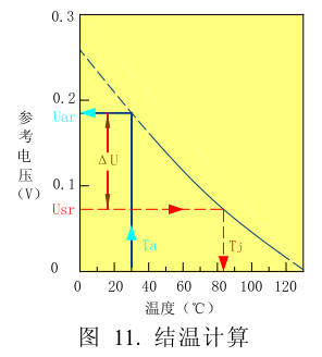
1 The methods for testing Ua, Us, and Ta are the same as those described in the previous section.
2 Calculate ΔU=Ua-Us ;
3 find the corresponding point in the K curve according to the value of Ta, read the reference voltage value Uar;
4 Subtract ΔU from Uar value to get the corresponding reference voltage Usr, that is, Usr=Uar-ΔU
5 The horizontal line and the curve are intersected by the Usr value to obtain the corresponding temperature value. This temperature value is the junction temperature Tj of the thermal steady state during the test.
Note: The voltage on the ordinate of the given K-graph is only a relative reference value indicating each point on the curve. The value of the ordinate should not be directly related to the measured value of the thermal steady-state voltage to find the junction temperature! Using the calculation ΔU to get the junction temperature is correct. Also note that no additional ambient temperature is required at this time.
As an engineering application, when testing the LED junction temperature in a luminaire, several test methods can be selected:
a. It is recommended to test the junction temperature with a four-wire method for a selected LED in the fixture.
b. If, due to structural design constraints, there may be large differences in LED temperature estimates at different locations, it may be best to measure the junction temperature of the individual LEDs by drawing leads from the selected key positions of the LEDs.
c. If you want to save a little calculation, you can directly measure the total voltage of the series LED, then divide by the number of LED series to get the Us value of a single LED. However, there will be errors caused by differences in the wires and LEDs, but if there is a margin in the design of the luminaire, the introduced errors are generally acceptable.
d. For integrated packaged LEDs, the average value can only be estimated.
Chapter II Thermal Resistance Method Calculate Junction Temperature
The first quarter heat resistance method measures the basic principle of junction temperature
The thermal resistance method is used to calculate the junction temperature. The theoretical basis is based on the theory of one-dimensional heat conduction in Fourier. It is assumed that the heat of the PN junction reaches the temperature measurement point of the outer surface of the heat sink vertically through the one-dimensional heat conduction, and the isothermic surface of the temperature measurement point does not exceed the package temperature. The body, or the composition of the isothermal surface, does not involve radiative heat transfer. In this way, one can use Fourier's one-dimensional heat conduction formula to calculate. According to Fourier one-dimensional heat conduction theory:
P=Aλ(Tj-Tr)/L=AλΔT/L—(4)
In the formula:
P: One-dimensional heat flow from the PN junction to the surface of the heat sink;
Tj: junction temperature; Tr: reference point temperature;
A: Thermal conduction path cross-sectional area; L: path length
make:
R=L/(Aλ)—(5)
R is called the conduction thermal resistance.
Then formula (4) can be expressed as:
R = (Tj - Tr) / P = ΔT/ P - (6)
In fact, the heat generated by the PN junction is not one-dimensionally conducted, that is, the entire heat generated by the PN junction is not only conducted downward to the heat sink. In reality, one-dimensional heat conduction is rare. Therefore, when we apply thermal resistance to analysis and calculation, we often need to use the concept of equivalent thermal resistance. With the concept of equivalent thermal resistance, the concept of isothermal surface is often used. The equivalent thermal resistance between two isothermal surfaces is actually a result of many series and parallel thermal resistances.
Using the equivalent thermal resistance concept, the equivalent thermal resistance can still be calculated using the formula (6) in the case of only thermal conduction and thermal convection. However, if the heat transfer within the isothermal plane involves radiative heat transfer, the form of equation (6) no longer holds. Therefore, when measuring the thermal resistance of a device, the temperature measurement point on the surface of the device must be selected so that the isothermal surface where the change point is located does not involve radiative heat transfer. (Beyond the isothermal surface, there may be radiant heat transfer.)
Only when the isotherm of the device temperature measurement point does not exceed the package (this prerequisite must be satisfied), P can use the PN junction to generate the total thermal power value. Please refer to the literature [1] for the argument in this respect.
Transforming equation (6) yields:
Tj=Tr+PR—(7)
Equation (7) is the formula for calculating the junction temperature by the thermal resistance method in normal engineering.
From Equation (7), to calculate the junction temperature, we must first know the thermal resistance R of the device.
How do you know the thermal resistance?
æ ¹æ®ä¸Šé¢æ‰€è¿°ï¼Œé€šå¸¸æƒ…况下都ä¸å¯èƒ½æ˜¯ä¸€ç»´çƒä¼ 导,就ä¸èƒ½ç”¨å…¬ç¤ºï¼ˆ2)æ¥è®¡ç®—çƒé˜»ï¼Œå› æ¤ï¼Œå¯¹äºŽå™¨ä»¶çš„çƒé˜»ï¼Œä¹Ÿåªèƒ½æ˜¯é‡‡ç”¨ç‰æ•ˆçƒé˜»ã€‚当然,如果概念清楚的è¯ï¼Œæˆ‘们还å¯ä»¥ç®€åŒ–用“çƒé˜»â€ä¸€è¯ã€‚该ç‰æ•ˆçƒé˜»çš„测温点选择必须满足上é¢æ‰€è®²åˆ°çš„“å‰ææ¡ä»¶â€ã€‚实际上,器件的çƒé˜»å€¼æ˜¯æ ¹æ®ç”µåŽ‹æ³•æ¥æµ‹ç®—得到的。
具体求得çƒé˜»å€¼çš„æ¥éª¤å¦‚下:
①利用电压法,首先测出器件的K 系数。
â‘¡ 将器件在æŸä¸ªæ•£çƒç»“æž„ä¸‹å·¥ä½œï¼Œåˆ©ç”¨ç¬¬ä¸€ç« ç¬¬ä¸‰èŠ‚çš„æ–¹æ³•æµ‹ç®—å‡ºçƒç¨³æ€ä¸‹çš„结温。
â‘¢ æ ¹æ®å™¨ä»¶çš„çƒåŠŸçŽ‡å€¼ï¼Œåˆ©ç”¨å…¬å¼ï¼ˆ6)算出çƒé˜»å€¼ã€‚
â‘£ å™¨ä»¶ç”¨æˆ·æ ¹æ®å™¨ä»¶åŽ‚商给出的çƒé˜»å€¼ï¼Œåœ¨å®žé™…器件使用的状æ€ä¸‹ï¼Œé€šè¿‡æµ‹è¯•å™¨ä»¶æµ‹æ¸©ç‚¹çš„温度,利用公å¼ï¼ˆ7)æ¥ç®—出结温。
通常,å‰é¢ä¸‰æ¥æ˜¯ç”±å™¨ä»¶åŽ‚商完æˆï¼Œç¬¬â‘£æ¥æ˜¯ç”±å™¨ä»¶ç”¨æˆ·æ“作完æˆã€‚通常人们所知的çƒé˜»æ³•æµ‹ç»“温,往往åªæ˜¯è°ˆåŠç¬¬â‘£æ¥ï¼Œå®žé™…上,çƒé˜»æ³•æµ‹ç»“温的完整æ¥éª¤åº”该是包括上述四个æ¥éª¤çš„。没有å‰é¢çš„三个æ¥éª¤ï¼Œç¬¬å››æ¥å°±æ— 从谈åŠã€‚
从上é¢çƒé˜»æ³•çš„测算结温的原ç†å¯ä»¥çœ‹åˆ°ï¼Œçƒé˜»æ³•æµ‹ç®—结温,其实是电压法的一ç§å»¶ä¼¸æˆ–å˜é€šã€‚
我们å¯ä»¥çœ‹åˆ°ï¼Œåœ¨çƒé˜»æ³•çš„全部æ¥éª¤ä¸ï¼Œå‰ä¸¤æ¥çš„方法已ç»å¯ä»¥å¾—到结温值了,å³åˆ©ç”¨ç”µåŽ‹æ³•å·²ç»å®Œå…¨å¯ä»¥è§£å†³é—®é¢˜äº†ã€‚利用结温去算出一个çƒé˜»å€¼ï¼Œå†åˆ©ç”¨çƒé˜»å€¼åŽ»ç®—结温(看起æ¥åƒæ˜¯åœ¨è½¬åœˆåœˆï¼‰ï¼Œçƒé˜»æ³•çœ‹èµ·æ¥æ˜¯ä¸€ç§å¤šä½™çš„åšæ³•ã€‚为什么还è¦æœ‰çƒé˜»æ³•ï¼Ÿä¸‹é¢è§£é‡Šã€‚
第二节çƒé˜»æ³•æµ‹ç»“温的问题
1. 为什么è¦ç”¨çƒé˜»æ³•æµ‹ç»“温
在数å—表出现之å‰è¿˜æ˜¯é‡‡ç”¨æŒ‡é’ˆå¼ç”µåŽ‹è¡¨ï¼Œå®ƒçš„æŒ‡é’ˆè¿‡å†²é€ æˆæ— 法准确读到瞬时数æ®ã€‚è¦å‡†ç¡®æµ‹é‡ç”µåŽ‹ï¼Œéœ€è¦ç²¾å¯†çš„电压表。这ç§ç²¾å¯†ä»ªè¡¨ä¸€èˆ¬ä»·æ ¼å¾ˆè´µï¼Œå¯¹ä¸€èˆ¬ç”¨æˆ·è€Œè¨€ï¼Œä¸ä¼šå› 为很少的使用而去è´ä¹°ã€‚所以æ‰ä¼šæœ‰å…ƒä»¶åŽ‚给出çƒé˜»å€¼æ–¹ä¾¿ç”¨æˆ·ç”¨æµ‹é‡å‚考点的温度æ¥è¿‘似计算结温的åšæ³•ã€‚
å› ä¸ºæ¸©åº¦è®¡å®¹æ˜“å¾—åˆ°ã€‚è¿™å°±æ˜¯çƒé˜»æ³•å˜åœ¨çš„åŽŸå› ã€‚
从çƒé˜»æ³•çš„原ç†æˆ‘们å¯ä»¥çœ‹åˆ°ï¼Œçƒé˜»æ³•ç¦»ä¸å¼€ç”µåŽ‹æ³•ã€‚è¦æ±‚å¾—çƒé˜»ï¼Œå¿…å…ˆè¦æµ‹å¾—K 系数。有了K系数,å†åˆ©ç”¨ç”µåŽ‹æ³•å°±å¯ä»¥æµ‹ç®—结温了。å‰ææ¡ä»¶æ˜¯ï¼Œè¦æœ‰ä¸ªé«˜ç²¾åº¦çš„电压表。现在能满足电压法测试精度的数å—电压表很普éï¼Œä»·æ ¼ä¹Ÿå¾ˆä½Žã€‚ç”µåŽ‹æ³•çš„æ™®åŠåº”用ä¸æ˜¯é—®é¢˜äº†ã€‚而且在实际的应用æ“作ä¸ï¼Œæµ‹ç”µåŽ‹æ¯”测温度è¦æ–¹ä¾¿çš„多ï¼
举例æ¥çœ‹ã€‚比如一个集æˆå°è£…çš„LED å…‰æºï¼Œæ£ç¡®çš„çƒé˜»å‚考点应该是çƒæ²‰åº•éƒ¨ä¸å¤®ã€‚实际应用时,光æºè¦æŽ¥æ•£çƒå™¨ï¼Œé‚£ä¹ˆå‚考点的温度如何测?必须在散çƒå™¨ä¸Šæ‰“å”(有关åŠå¯¼ä½“器件çƒé˜»æµ‹è¯•çš„æ£ç¡®æ–¹æ³•è¯»è€…å¯ä»¥å‚çœ‹æœ‰å…³æ ‡å‡†ï¼‰ã€‚è€Œç”¨æµ‹ç”µåŽ‹çš„æ–¹æ³•ï¼Œä¸éœ€å¯¹ç¯å…·åšç ´å,简å•æ˜“行。
2. çƒé˜»å‚考点的选择
çƒé˜»æµ‹æ¸©å‚考点的选择是很é‡è¦çš„,如果选择ä¸æ£ç¡®ï¼Œå¾—到的çƒé˜»å€¼å°†ä¸å…·æœ‰å®žç”¨æ€§ã€‚并且有关计算在ç†è®ºä¸Šå¯èƒ½éƒ½æ˜¯é”™è¯¯çš„。也就是说,测温点选择ä¸æ£ç¡®ï¼Œæ‰€åšçš„一切都是错误的。这方é¢çš„论è¯è¯·å‚看文献ã€1】。器件的çƒé˜»å€¼æµ‹æ¸©å‚考点通常应该是:PN 结到å°è£…壳体çƒæ²‰å¤–表é¢æœ€è¿‘è·ç¦»çš„ä½ç½®ã€‚
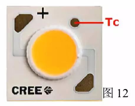
在LED æ–¹é¢ï¼Œæ¸©åº¦å‚考点选择错误的现象比比皆是。比如:éšæ„选择电æžç„Šç‚¹ä½œä¸ºæ¸©åº¦æµ‹è¯•ç‚¹ï¼›ä¸€äº›é›†æˆå°è£…å’ŒCOB å°è£…çš„LED 产å“,将温度测试点选择在å‘å…‰é¢ä¸€ä¾§ï¼Œè€Œä¸æ˜¯åœ¨çƒæ²‰ä¸Šï¼Œå‚看图12,这是错误的。以æ¤ç‚¹ä½œä¸ºå‚考点,å†åˆ©ç”¨å…¬å¼ï¼ˆï¼•ï¼‰å’Œï¼ˆï¼–)时,ç†è®ºä¸Šå°±æ˜¯é”™è¯¯çš„。
3. å™¨ä»¶ä¼ çƒçŠ¶å†µçš„å½±å“
利用çƒé˜»æ³•æµ‹ç®—结温,必须考虑器件çƒé‡çš„ä¼ é€’çŠ¶å†µã€‚æ ¹æ®çƒé˜»æ³•æ‰€ä¾æ®çš„计算公å¼ï¼ˆ4)æ¥çœ‹ï¼Œè¯¥å…¬å¼çš„å½¢å¼åªé€‚åˆäºŽä¼ 导和对æµã€‚如果测试å‚考点的ç‰æ¸©é¢æ¶‰åŠåˆ°è¾å°„,由于è¾å°„ä¼ çƒä¸Žæ¸©åº¦çš„关系ä¸æ˜¯çº¿æ€§å…³ç³»ï¼Œä¸å˜åœ¨å…¬å¼Pï¼Î”T/R çš„å½¢å¼ï¼Œæ‰€ä»¥å†åˆ©ç”¨å…¬å¼ï¼ˆ5)就是错误的。器件的çƒé‡å¿…é¡»å…¨éƒ¨ä»¥ä¼ å¯¼ã€æ¶²ä½“对æµçš„æ–¹å¼ä¼ 递到å‚考点。注æ„:必须是液æ€æµä½“对æµï¼ˆå¯¹æ¶²ä½“对æµæ¢çƒï¼Œå›ºã€æ¶²ç•Œé¢çš„ç‰æ¸©é¢ä¸Šï¼Œå…¬å¼Pï¼Î”T/R çš„å½¢å¼ä¾ç„¶æˆç«‹ï¼‰ï¼Œè€Œä¸æ˜¯ç©ºæ°”ã€‚å› ä¸ºæ¸©åº¦å‚考点如果æ›éœ²äºŽç©ºæ°”ä¸ï¼Œåˆ™å¯èƒ½å˜åœ¨è¾å°„ä¼ çƒçš„情形。
4. 温度的影å“
å‰é¢è®²åˆ°ï¼Œä¸€èˆ¬LED çš„K 系数都ä¸æ˜¯çº¿æ€§çš„,而是éšæ¸©åº¦å˜åŒ–的。由æ¤å¯çŸ¥ï¼Œçƒé˜»å€¼ä¹Ÿæ˜¯éšæ¸©åº¦å˜åŒ–的。所以,器件厂商给出一个çƒé˜»å€¼ï¼Œæ˜¯åœ¨ä»€ä¹ˆæ¸©åº¦ä¸‹æµ‹è¯•çš„?如果ä¸æ˜Žç¡®ï¼Œæˆ–å³ä½¿ç»™å‡ºä¸€ä¸ªæµ‹è¯•æ¸©åº¦ï¼Œä½ 在实际应用器件时的温度是å¦ç¬¦åˆè¿™ä¸ªæ¸©åº¦è¦æ±‚?如æ¤ä¸€æ¥ã€‚准确性何言?
5. çƒé˜»æ³•æµ‹ç»“温å‚考点的æ£ç¡®é€‰æ‹©
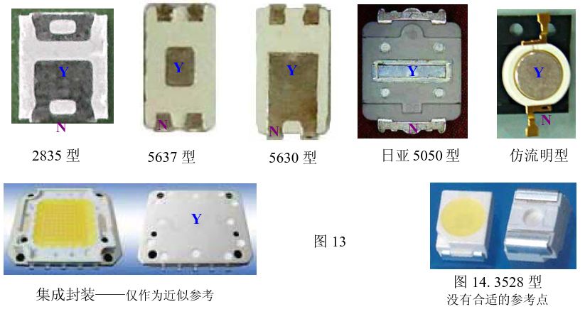
如果一定è¦é‡‡ç”¨çƒé˜»æ³•æ¥è®¡ç®—结温,应该æ£ç¡®é€‰æ‹©å°è£…体外表é¢çš„测温å‚考点。下é¢ç»™å‡ºä¸€äº›LED å°è£…体的å‚考点选择例。图13 ä¸â€œYâ€è¡¨ç¤ºæ£ç¡®çš„å‚考点,“Nâ€è¡¨ç¤ºé”™è¯¯çš„å‚考点。从这些例åæ¥çœ‹ï¼Œåœ¨å®žé™…ç¯å…·ä¸è¦æµ‹è¯•è¿™äº›ç‚¹çš„温度是ä¸å®¹æ˜“的,需è¦å¯¹PCB 或散çƒå™¨æ‰“å”æ‰è¡Œã€‚对于一些LED å°è£…体,å¯èƒ½ä¸å˜åœ¨çƒé˜»æ³•æ‰€éœ€çš„å‚考点。对于这类å°è£…çš„LED,åªèƒ½é‡‡ç”¨ç”µåŽ‹æ³•æ¥æµ‹ç®—结温。例如图14。
ç¬¬ä¸‰ç« å…¶å®ƒæµ‹ç»“æ¸©æ–¹æ³•ç®€ä»‹
现在还出现了一些其它测é‡LED 结温的方法。但是这些方法è¦ä¹ˆæ˜¯å‡†ç¡®æ€§æ–¹é¢å˜åœ¨é—®é¢˜ï¼Œè¦ä¹ˆæ˜¯éœ€è¦æ˜‚贵的仪器。ä¸é€‚åˆä¸€èˆ¬å™¨ä»¶ä½¿ç”¨è€…实际应用。下é¢ç®€å•ä»‹ç»ã€‚
1. å…‰è°±æ³•ï¼šæ ¹æ®LED 的光谱éšæ¸©åº¦çš„å˜åŒ–æ¥æµ‹ç®—结温。 è¿™ç§æ–¹æ³•ï¼Œä¸€èˆ¬åªèƒ½ä¸“业测试机构拥有。而且这ç§æ–¹æ³•å¯¹ä»ªå™¨çš„精度è¦æ±‚很高。
2. è“ç™½æ³•ï¼šæ ¹æ®ç™½å…‰å…‰è°±èƒ½é‡å’Œè“光光谱能é‡çš„比值与温度的关系æ¥æ±‚结温。
è¿™åªé€‚åˆç™½å…‰LED,且也åªèƒ½ä¸“业测试机构拥有。
3. 红外光谱æˆåƒæ³•ï¼š è¿™ç§æ–¹æ³•å®žé™…是ä¸èƒ½æµ‹åˆ°ç»“温的。å³ä½¿æ˜¯æœªå°è£…的芯片,测得的也åªæ˜¯èŠ¯ç‰‡è¡¨é¢æ¸©åº¦ï¼Œè€Œä¸æ˜¯å†…部的结温。
è¿™ç§æ–¹æ³•å¯ä»¥å¯¹æŸæ¬¾èŠ¯ç‰‡åšæµ‹è¯•ï¼Œç„¶åŽä¸Žç”µåŽ‹æ³•æµ‹å¾—的结果对比求得一个æ¢ç®—系数。但是,对ä¸åŒçš„芯片或å°è£…,ä¸å…·æœ‰é€šç”¨æ€§ã€‚å³è¿™æ¬¾èŠ¯ç‰‡å’Œå°è£…的器件的æ¢ç®—系数,å¯èƒ½æ˜¯ä¸é€‚åˆä¸åŒèŠ¯ç‰‡å’Œå°è£…的。
å› æ¤ï¼Œä¸¥æ ¼è®²ï¼Œçº¢å¤–法ä¸é€‚宜åšå‡†ç¡®æµ‹é‡ç»“温用,åªé€‚åˆåšçƒåˆ†æžç”¨ã€‚
è“白法本质上也是光谱法。这两ç§æ–¹æ³•å¯¹æµ‹è¯•ä»ªå™¨çš„è¦æ±‚éƒ½å¾ˆé«˜ï¼Œä»ªå™¨ä»·æ ¼æ˜‚è´µï¼Œåªé€‚åˆå®žéªŒå®¤ç ”究用。ä¸é€‚åˆä¸€èˆ¬ç¯å…·åŽ‚商开å‘ç¯å…·äº§å“ä½¿ç”¨ã€‚å› ä¸ºä¸€æ¬¾ç¯å…·çš„å¼€å‘,ä¸å¯èƒ½ä¸€æ¬¡è®¾è®¡ã€ä¸€æ¬¡åšæ ·å°±æˆåŠŸï¼Œå¾€å¾€éœ€è¦å¤šæ¬¡è¯•éªŒã€‚ä¸å¯èƒ½å¯¹æ¯æ¬¡è¯•éªŒçš„æ ·å“都é€åˆ°æµ‹è¯•æœºæž„用昂贵的仪器ã€å¾ˆé«˜çš„费用去测试结温的状况。
光谱法用æ¥ç ”究LED 的光谱与结温的关系ã€ä½œä¸ºæŽ¢ç©¶ã€äº†è§£LED 的特性是å¯ä»¥çš„ï¼Œä½†ä½œä¸ºä¸€èˆ¬å·¥ç¨‹ä¸Šæµ‹ç»“æ¸©å¹¶æ— å¿…è¦ã€‚å› ä¸ºç”µåŽ‹æ³•ç®€ä¾¿ã€å‡†ç¡®ï¼Œä¸”廉价。
in conclusion
1. 测é‡LED 的结温,电压法是最简å•æ˜“è¡Œã€å‡†ç¡®åº¦æœ€å®¹æ˜“ä¿è¯ã€æµ‹è¯•æˆæœ¬æœ€ä½Žçš„方法。
2. çƒé˜»æ³•åœ¨å®žé™…应用ä¸å˜åœ¨å¾ˆå¤šé—®é¢˜ï¼Œå¾ˆå¤šäººä¸äº†è§£çƒé˜»æ³•æµ‹è¯•å¿…é¡»éµå¾ªçš„ç†è®ºä¾æ®ï¼Œå®žé™…æ“作ä¸é”™è¯¯åœ°é€‰æ‹©æµ‹æ¸©ç‚¹å¯¼è‡´ç»“果错误。建议淘汰。
Monochrome Lcd-Cog,Graphics Lcd Display,Transmissive Cog Lcd Module,Positive Cog Lcd Module
Huangshan Kaichi Technology Co.,Ltd , https://www.kaichitech.com