Miniaturization, integration and intelligence are an important trend in the development of modern science and technology. With the development of micro-electromechanical processing system (MEMS) technology, electronic computers have evolved from the "big beast" to a portable system composed of tiny circuit integrated chips, and even a miniature smart phone.
The MEMS technology is called Micro Electromechanical System. The MEMS idea was proposed by Richard Feynman, the Nobel Prize winner in Physics, in 1959. The basic concept is to use semiconductor technology to miniaturize the mechanical system in real life to form a micro-electromechanical system. Abbreviated as MEMS.
In 1962, the world's first miniature pressure sensor was introduced. This innovative product was later applied to automotive safety (tire pressure detection) and medical treatment (invasive sphygmomanometer) and opened the MEMS era. Today, MEMS technology plays a key role in the military, aerospace, biomedical, industrial transportation, and consumer sectors. In smart phones, multiple MEMS chips are embedded, such as microphones, accelerometers, and GPS positioning.
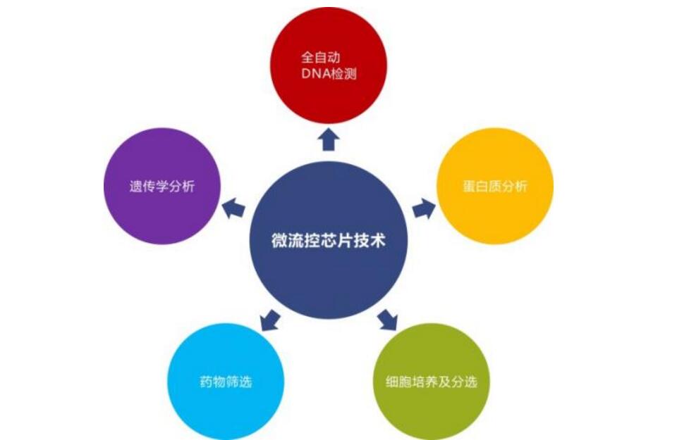
Microfluidics (microfluidics) is a scientific technology that precisely controls and manipulates microscale fluids and manipulates fluids in micro- and nano-scale spaces. It has the basic functions of biological and chemical laboratories such as sample preparation. The ability to react, separate, and inspect microscopically to a few square centimeters on a chip. The basic features and greatest advantages are the flexible combination and scale integration of multiple cell technologies on an overall controllable micro-platform. It is an interdisciplinary discipline that covers engineering, physics, chemistry, microfabrication and bioengineering.
Microfluidics is the scientific science of the system. It uses tens to hundreds of micron-scale pipelines to process or manipulate very small (10* to 10 to 18 liters, 1 to 3 cubic millimeters to 1 cubic micron) fluids. The original microfluidic technology was used for analysis. Microfluidics provides many useful functions for analysis: Using very few samples and reagents to make high-precision and high-sensitivity separations and detections, with low cost, short analysis time, and small footprint of analytical equipment. Microfluidics utilizes both its most obvious features, small size and the use of less obvious microchannel fluid characteristics, such as laminar flow. It essentially provides the ability to centrally control molecules in space and time.
1. The microfluidic analysis chip is a new generation of point-of-care testing (POCT) mainstream technology that can provide fast and effective biochemical indicators directly around the subject to be tested, making on-site testing, diagnosis, and treatment a continuous process. ;
2. The microfluidic reaction chip, represented by droplets, is by far the most important microreactor, and shows great power in high-throughput drug screening, single cell sequencing and other fields;
3. The microfluidic cell/organ manipulation chip is the most important technology platform for manipulation of mammalian cells and their microenvironment. It is eager to partially replace animal models such as mice to verify candidate drugs and develop drug toxicology and pharmacological effects.
The traditional lithography and etching techniques used to fabricate semiconductors and integrated circuit chips are the most basic of microfluidic chip processing technology. It is micro-processed with phototool, mask, and ultraviolet light. The process is mature and has been widely used to fabricate microstructures on silicon, glass, and quartz substrates. Lithography and etching techniques consist of three processes: thin film deposition, photolithography, and etching. The complex microstructure can be completed by repeating the three steps of thin film deposition - photolithography.
Before the lithography, the surface of a clean substrate is covered with a film, and the thickness of the film is several angstroms to several tens of micrometers. This process is called film deposition. Thin films can be divided into epitaxial layers in the working area of ​​the device, masking films that limit the area expansion, insulating dielectric films that function as protection, passivation, and insulation, and can be used as conductive metal films for electrode bonding and wire interconnection. Commonly used membrane materials are silicon dioxide, silicon nitride, boro-phospho-silicate glass, polysilicon, conductive metals, lithographic resists, and refractory metals. The main methods for manufacturing processed films are oxidation, chemical vapor deposition, evaporation, sputtering, and the like.
A layer of photo-resist is evenly covered on the surface of the film, and the process of transferring the micro-fluid-control chip design pattern on the mask to the photo-resist layer through the principle of exposure imaging is called photolithography. Lithography generally consists of the following basic processes:
1. Pretreatment of the substrate.
The surface of the substrate is cleaned by degreasing, polishing, pickling, and washing to ensure good adhesion of the photoresist to the surface of the substrate.
2. Apply glue
The treated substrate surface is evenly coated with a layer of photo-resist having good adhesion and thickness. The film is too thin, it is easy to generate pinholes, and the anti-corrosion ability is poor; if it is too thick, it is not easy to develop completely, and at the same time it will reduce the resolution. The actual thickness of the photoresist is related to its viscosity and is inversely proportional to the square root of the spin speed of the spin-off machine. The coating methods include a spin coating method, a brush coating method, a dipping method, and a spray coating method.
3. Pre-baking
At a certain temperature, the solvent in the photoresist solution is volatilized to enhance the adhesion of the photoresist and the substrate and the abrasion resistance of the film. The temperature and time of the prebaking are determined by the type and thickness of the photoresist. Electrothermal thermostats, hot air or infrared heat sources are often used.
The prebaking temperature and time should be appropriate. If the temperature is too high or the time is too long, it will cause the bottom film or the photosensitivity to decrease when developing, and the island will appear when the corrosion occurs; if the temperature is too low or the time is too short, it will cause the pin hole after development. Increase, or produce floating plastic, graphics deformation and so on.
4. Exposure
A lithography mask prepared with a desired chip pattern is overlaid on the substrate, and the photoresist is selectively irradiated through a mask using ultraviolet rays or the like. Photoresist irradiated by light chemically reacts.
In actual operation, the exposure time is determined by the photolithography film, film thickness, light source intensity, and the distance between the light source and the substrate. Exposure methods include chemical exposure, contact and proximity copy exposure, and optical projection imaging exposure.
5. Development
The exposed adhesive (non-optical adhesive) or unexposed adhesive (negative adhesive) is chemically removed by a photo-complementary developer solution, and the choice of developer and development time has a great influence on the development effect. The principle of choosing a developer is that the part of the film that needs to be removed has a large solubility, a high dissolution rate, and a small solubility in the part that needs to be retained. The development time varies depending on the type of photoresist, film thickness, type of developer, development temperature, and operation method.
6. Hard film
After the developed substrate is cleaned and baked at a certain temperature, the solvent or moisture remaining in the film after development is completely removed, so that the adhesive film and the substrate are closely adhered to prevent the adhesive layer from peeling off, and the adhesive film is reinforced. Its own corrosion resistance. The hardening temperature and time should be appropriate.
Etching is a process of transferring a planar two-dimensional pattern on a photo-resist layer onto a thin film and further processing it into a certain depth of micro-structure on the substrate.
According to different etching state, the etching process can be divided into wet etching and dry etching. Wet etching is an etching method that peels off an etched substance by a chemical reaction between a chemical etching solution and an etched substance. Most wet etching is isotropic etching that is not easy to control.
Its characteristics are high selectivity, good uniformity, and less damage to silicon wafers. It is suitable for almost all metals, glass, plastics and other materials. The disadvantage is that the fidelity of the picture is not strong. At the same time as lateral etching, lateral undercutting often occurs, so that the minimum line width of the etching pattern is limited.
Dry etching refers to a process in which a high-energy beam reacts with a surface film to form a volatile substance or directly bombards the surface of the film to be corroded. The most important feature is that it can achieve anisotropic etching, that is, the etching rate in the longitudinal direction is much greater than the rate of lateral etching, so as to ensure the fidelity after the transfer of the fine patterns. The role of dry etching is based on the plasma.
When photolithography is used to process microfluidic chips, photolithography masks must first be fabricated. The basic function of the mask is that when the substrate is exposed to a light beam, different light absorption and transmission capabilities are created in the graphics area and the non-graphic area. The computer graphics system is used to convert the mask patterns into data files. The dedicated interface circuit is used to control the exposure light source, iris diaphragm, worktable and lens in the pattern generator to make the desired pattern on the mask material. Or use a computer to convert the structure diagram of the design microchannel into an image file through CAD software, and print the image on a transparent film with a high-resolution printer. This transparent film can be used as a mask for lithography, which can basically meet the requirements of the microfluidic chip for the mask.
(2) hot pressingHot-pressing (hot-embossing) is a kind of widely used chip manufacturing technology for rapid copying of electrophoretic microchannels. It is suitable for thermoplastic polymer materials such as PMMA and PC. The hot-pressing method can be a metal wire with a diameter of less than 50um or a micro-channel bone film etched with a protrusion, such as a nickel-base male mold, a single-crystal silicon anode mold, a glass male mold, and a micro-machined metal. Positive model. This method can be copied in large quantities, the equipment is simple and the operation is simple, but the materials used are limited.
(3) MoldingLithography and etching are used to make the positive mold first (the desired channel part is projected); the liquid polymer material is poured, and then the solidified polymer material is peeled from the positive mold to obtain the micro-channel chip. The chip method is called molding. The key to molding is the choice of molds and polymer materials. The ideal materials should have low adhesion to each other and be easily demoulded.
The microchannel positive film can be made of silicon material, glass, epoxy SU-8 negative photoresist, PDMS, and the like. Silicon or glass cations can use standard etching techniques. The PDMS mold can be made by direct casting on a master mold made of a silicon material, glass, or the like.
Pouring polymer materials should have low viscosity and low curing temperature. Under the action of gravity, the microchannels and grooves on the mold can be filled. There are two types of materials available: curable polymers and solvent-volatile polymers.
Although the molding method is limited to polymer materials, the method is simple, the chip can be mass-reproduced, and does not require expensive equipment. It is a method that can produce inexpensive analysis chips.
(4) Injection moldingThe process of the injection molding process is to etch the negative mold of the electrophoresis chip on the silicon wafer through photolithography and etching techniques. The negative mold is electroformed for about 24 hours to obtain a 0.5-cm-thick nickel alloy mold, and then the nickel alloy mold is added. Thick and carefully machined into metal injection molds, this mold is mounted on an injection molding machine to mass produce polymer microfluidic chip substrates.
In the injection molding process, mold making is complex, technical requirements are high, and the cycle is long, which is a key step in the entire process. A good mold can produce 300,000 to 500,000 polymer chips, which has good repeatability, short production cycle, and low cost, and is suitable for the production of molded chips.
(5) LIGA technologyLIGA is the abbreviation of the German word Lithographie, Galvanoformung, Abformung. LIGA technology is composed of three links: lithography, electroforming and plastic casting.
The quasi-LIGA technology uses an ultraviolet light source to replace the synchrotron radiation X-ray deep lithography in the LIGA technology, and then performs a subsequent micro-electroforming and micro-replication process. It does not require synchrotron radiation X-ray lithography and a special X-ray mask, which is conducive to mass production of micro-mechanical devices. According to the different process routes of UV deep lithography, quasi-LIGA technology can be divided into three categories: multi-layer lithography-LIGA, silicon-mode deep etch-LIGA and SU-8 deep-lithography-LIGA.
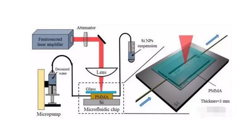
(6) Laser AblationLaser ablation is a non-contact microfabrication technique. It can directly process complex microstructures on metals, plastics, ceramics and other materials based on computer CAD data, and has been applied to micro-mode and micro-channel processing. This method requires high technical equipment, simple steps, and does not require ultra-clean environment, high precision. However, due to the large UV laser energy, there is a certain
Danger, need to operate in the standard laser lab, use safety equipment and protective glasses.
(7) Soft LithographySoft lithography (softlithography) is a new approach to micropattern transfer and microfabrication relative to the dominant lithography in microfabrication, based on self-assembled monolayers, elastomeric stamps, and polymer molding technology New microfabrication technology. It can produce complex three-dimensional structures and irregular surfaces; it can be applied to many kinds of materials such as biopolymers, colloids, glass, ceramics, etc. Without the precision limitations associated with the scattering, it can reach the tiny size of 30nm~1um; therefore, it is soft. Lithography is a cheap, convenient technology that is suitable for laboratory use.
The core of soft lithography technology is the elastic stamp, which can be obtained by photolithography and molding. PDMS is the most commonly used elastic die seal in soft lithography. The key technologies of soft lithography mainly include microcontact printing, remolding, micro-transfer molding, capillary molding, and solvent assisted molding.
The soft lithography technology still has some defects, such as 1% shrinkage deformation of PDMS after curing, and under the action of toluene and ethane, the aspect ratio will have a certain expansion; the elasticity and thermal expansion of PDMS make it difficult Obtaining high accuracy also makes soft lithography limited in multi-layer micromachining; because the elastic modulus is too soft, a large aspect ratio cannot be obtained, and the ratio of width to depth that is too large or too small will lead to microstructures. Distorted or distorted.
With Yuchai Engine Diesel Generator
With Yuchai Engine Diesel Generator,Yuchai Diesel Generator,Yuchai Diesel Generator Set,Yuchai Generator
Shanghai Kosta Electric Co., Ltd. , https://www.ksdpower.com