This article introduces the design of multi-channel data acquisition and storage system consisting of TMS320F2812 and ADS8365.
Introduction to TMS320F2812TMS320F2812 is a TI high-performance TMS320C28x series 32-bit fixed-point DSP processor. TL2812-EVM is a high-performance DSP development board based on TI TMS320F2812. It adopts core board + backplane mode, size is 185mm*135mm, and the bottom board adopts sinking. The two-layer board design of the gold lead-free process provides users with a test platform for the SOM-TL2812 core board for rapid evaluation of the overall performance of the core board.
TI's main performance TMS320C28x series TMS320F2812 32-bit fixed-point micro-control unit (MCU), clocked at up to 150MHz; with I2C, SPI, CAN, PWM and other bus interfaces, suitable for a variety of control industrial equipment; small size, high performance, portable High performance, suitable for a variety of handheld devices; meets high and low temperature, vibration testing, to meet industrial environmental applications.
Introduction to ADS8365The ADS8365 is a high speed, low power, 6 channel simultaneous sampling and conversion, single +5V powered analog to digital conversion chip. Converts a maximum sampling throughput of up to 5MHz with a full-interpolation input channel with 80dB common-mode rejection and six differential sample-and-hold amplifiers. The pin also has a 2.5V reference and a high speed parallel interface.
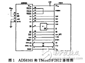
Interface design of hardware design of synchronous data acquisition system TMS320F2812 and ADS8365The data readout of the ADS8365 can be directly address read, FIFO read, or cyclic read. Therefore, there are at least three interconnection schemes for the interface with the TMS320F2812. The acquisition system selects the direct address read mode, and XA[2:0] is used as the lower address of the conversion result register. When the CS pin of the ADS8365 is high, its data bus is in a high-impedance state. When the CS pin is set low, The current data is output on the parallel port data bus. The specific connection circuit is shown in Figure 1.

The ADS8365 can use a separate external crystal or use the TMS320F2812I/O port to simulate a crystal. This system uses the T1PWM of the TMS320F2812EVA to generate the CLK clock input signal for the ADS8365. In order to achieve simultaneous sampling of six channels, the GPIOB14 pin of the TMS320F2812 is connected to the HOLDA, HOLDB, and HOLDC signals of the ADS8365 to control the synchronization of the three ADC sample/hold modules. The EOC is connected to the XINT1 of the TMS320F2812.
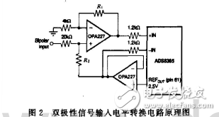
To form a multi-channel data acquisition such as 12/24, the CS address expansion of the ADS8365 can be performed using the lower address line of the TMS320F2812. The remaining signals such as CLK and HOLDX can be connected to the above control signal line. In this system, the voltage signal output by the sensor is ±5V, and the analog input of the ADS8365 chip can receive ±2.5V. Therefore, the signal is adjusted by the power amplifier circuit in the front end of the ADS8365. This paper uses OPA227. The chip is implemented. The schematic is shown in Figure 2.

Figure 2 Bipolar signal input level conversion circuit schematic diagram OPA227 is a high precision, low noise operational amplifier produced by TI, with 8MHz bandwidth, open loop gain up to 160dB, bias voltage 75μV, can be applied to signal acquisition and In communication equipment. The lower OPA 227 in Figure 2 is a follower circuit that provides a reference voltage of 2.5V; the upper OPA 227 is used to implement level signal operations. In practical applications, an OPA227 should be added to the input to increase the input impedance and enhance the anti-interference ability of the system. In the figure, R1 and R2 select 2k and 10k precision resistors with small temperature drift.
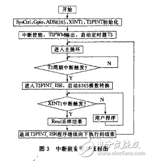
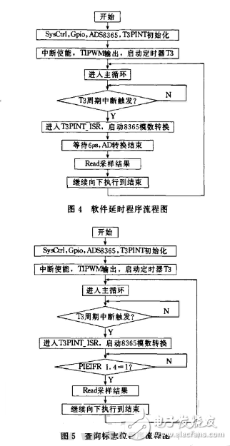
Data acquisition system software designThe TMS320F2812 chip provides a good C language development environment. Using C language shortens the development cycle and reduces the complexity of programming. The program flow chart is given below. The execution sequence of the program can be seen from the flow chart: First, after power-on, the ADS8365 is reset by hardware, the TMS320F2812 is initialized, and the corresponding system main frequency and the high-speed peripheral clock frequency related to sampling are set; Configure the Gpio port of the event manager used by the TMS320F2812 and the AD conversion chip; finally initialize the interrupt vector table, place the entry address of the Adc_isr() acquisition interrupt service routine at the vector address corresponding to the EOC input pin XINT, and configure it to The interrupt is triggered by a low level, and finally the system interrupt is enabled, waiting for the EOC interrupt signal to arrive.


Triggering the reset pin of the ADS8365 ensures that the read pointer points to the first data location. As part of the TMS320F2812 initialization, the GPIOF1 pin of the TMS320F2812 provides a reset signal to the RESET of the ADS8365. When the system clock is stable, RESET is triggered low, ensuring that the data output from the ADC corresponds to channels A0, A1. The arrangement of B0, B1, C0, C1. The following is the reset reference procedure for the ADS8365:
Void ResetADS8365(void){
GpioDataRegs.GPFCLEAR.all=0x0001;
Asm("RPT#200||NOP");
GpioDataRegs.GPFSET.all=0x0001;}
3.2 Initialization of TMS320F2812
The initialization of TMS320F2812 includes system initialization, GPIO initialization and initialization of peripheral interrupts, which are described as follows:
(1) The initialization of the TMS320F2812 system includes the configuration of the watchdog, the configuration of the system and peripheral clocks, and the configuration of the on-chip RAM.
(2) Initialization of GPIO, in order to facilitate communication with ADS8365, TMS320F2812 configures some pins of GPIOA, GPIOB and GPIOF as general-purpose input and output ports. These include the external interrupt pin triggered by the EOC pin and the conversion clock pin required by the ADS8365. The reference program is as follows: void InitGpio(void)
{
EALLOW;
GpioMuxRegs.GPAMUX.all=0x0003;
GpioMuxRegs.GPADIR.all=0xFFFF;
GpioMuxRegs.GPEMUX.all=0x0003;
GpioMuxRegs.GPEDIR.all=0x0003;
GpioMuxRegs.GPEQUAL.all=0x0000;
GpioMuxRegs.GPFMUX.all=0x0000;
GpioMuxRegs.GPFDIR.all=0x0005;
EDIS;
}
(3) Initialization of peripherals and interrupts, configuration of maskable and non-maskable interrupts, so that system interrupts can find valid addresses. 3.3 Signal Sampling Procedure After the above configuration is completed, the T1PWM output signal is started to the CLK pin of the ADS8365. When the ADS8365 chip is ready, the sampling signal is started. The program is as follows:
Void ToggleHOLDx(int ​​channel)
{
GpioDataRegs.GPACLEAR.all=channel;asm("RPT#25||NOP");
GpioDataRegs.GPASET.all=channel;
}
After the above program is executed, the 6 channels of the ADS8365 start sampling at the same time. After the sampling is completed, the EOC pin is set low, triggering the external interrupt program of the TMS320F2812, and sequentially reading the 6 sampling signal storage registers of the ADS8365 in the interrupt program. And save to a pre-specified location, waiting for the main program to process. The procedure is as follows:
Void read_ADD()
{
CHA0_Data[idx]=*ptrCHA0;
CHA1_Data[idx]=*ptrCHA1;
CHB0_Data[idx]=*ptrCHB0;
CHB1_Data[idx]=*ptrCHB1;
CHC0_Data[idx]=*ptrCHC0;
Start system, GPIO, ADS8365, XINT1 initialize ADC_READY interrupt enable, T1PWM output enters the main loop, start sampling, wait for interrupt to end CHC1_Data[idx]=*ptrCHC1;}4 experimental result and waveform after ADS8365 sampling, conversion is finished, the chip The EOC pin is deasserted, and the X28 pin of the F2812 is deasserted, so that the interrupt handler is entered. The F2812 issues instructions to sequentially read data from the six registers of the ADS8365. From Figure 5 we can clearly see the complete process from the triggering of the ADS8365 to the F2812 reading data. design. Solved the key problem of synchronous sampling of physical quantities in the topic of "brushless doubly-fed motor control system". At the same time, the design scheme has wide application in motor control, multi-axis positioning system, multi-channel data acquisition, etc. It can meet the high precision and high real-time requirements of high-speed alternating voltage signal acquisition.
VGA Cable, VGA to VGA HD15 Monitor Cable SVGA M/M HD Cable Gold Plated Connectors Support 1080P Full HD for PC, HD TV, Projector, etc
Product Features
The VGA cable is widely used in VGA digital transmission mode connection, adapted to a variety of electronic devices 15PIN interface, such as computers, high definition DVD and computer monitors, projectors, high definition digital TV, rear projection, plasma TVs and other appliances Device cable.
Compatible with the resolution
VGA cable can automatically identify the resolution required to adjust the device to support 800 * 600/1024 * 768/1152 * 864/1280720/1280 * 768/1280 * 800/1280 * 9601280 * 1024/1360 * 768/1600 * 1200/1920 * 1080
Connectivity - VGA to VGA Cable Connector HD15 Male to Male.
[15-pin MALE VGA CABLE] Screw-in VGA cable with 15-pin male input and output for gaming, video editing and video projection.
[HIGH PERFORMANCE] Supports resolutions at 800x600 (SVGA), 1024x768 (XGA), 1600x1200 (UXGA), 1080p (Full HD), 1920x1200 (WUXGA), and up for high resolution LCD and LED monitors.
[FUNCTIONS] Links VGA-equipped computer to any display with 15-pin VGA port also known as RGB, DE-15, HD-15, DB-15, D-sub 15 and HDB-15, input and output.
[FERRITE CORES] The VGA to VGA cable equipped with ferrite cores that could minimize crosstalk, avoid electrical radiation interference and protect against electromagnetic interference (EMI) and radio frequency interference (RFI).
[SECURITY] The VGA cord engineered with molded strain relief connectors for durability, grip treads for easy plugging and unplugging, and finger-tightened screws for a secure connection.
Compute Cable,Notebook Cable,HDMI to VGA Cord,VGA Cable,HDMI Cable
UCOAX , https://www.jsucoax.com