High-power LEDs are favored by people for their high efficiency, pollution-free, long life and many other advantages. However, high-power LEDs require low-voltage, high-current driving power supplies. In order to highlight the advantages of high-power LEDs, it is required to have a driving power supply. Higher efficiency, higher power factor, and overvoltage, overcurrent, and overtemperature protection.
1 Principle and design
The circuit designed in this paper is mainly divided into three parts: EMI module, PFC converter and DC/DC converter. The EMI module adopts double-loop filtering to achieve better results. The Fairchild FAN6961 chip is used as the control chip of PFC converter. The Boost transform is used to improve the power factor. The DC/DC converter uses LLC resonance and uses FSFR2100 as the control device to achieve high efficiency. The basic structure is shown in Figure 1.
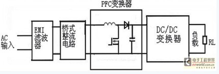
Figure 1 drive power design structure
1.1 EMI Module
The interference signal of the switching power supply can be divided into a common mode interference signal and a differential mode interference signal according to the conduction mode. The characteristics can be roughly divided into three frequency bands:
0.15~0.5MHz differential mode interference is dominant; 0.5~5MHz difference, common mode interference coexist; 5~30MHz common mode interference is dominant. At the time of design, if any frequency band is not up to standard, the filtering effect can be enhanced for this frequency band. For example, in the 0.15~0.5MHz frequency band, the suppression of the differential mode interference signal can be enhanced, the value of the capacitance Cx can be increased or the differential mode choke coil can be added; if the frequency range is not reached in the 5~30MHz frequency band, the suppression of the common mode interference signal can be enhanced. Increase the value of Cy or increase the number of stages of common mode filtering. When suppressing interference signals, the focus is on the suppression of common mode interference signals.

1.2 PFC converter design
1.2.1 How Boost Transformation Works
Boost converters are also known as parallel switching converters. When the control signal is turned on to turn on the switching transistor VT, energy is input from the input power source and stored in the inductor L. The diode VD is reverse biased, and the load is supplied by the filter capacitor C.
When VT is turned off, the current in the inductor L cannot be abruptly changed, and the induced potential generated by it prevents the current from decreasing, and the polarity of the potential is left-right and right-right. The diode VD is turned on, and the energy stored in the inductor flows into the capacitor C through the diode VD and is supplied to the load.
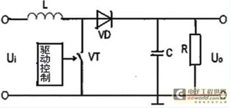
Figure 3 Boost converter circuit structure
1.2.2 Boost-based PFC converter design
We can see that during the conduction of the switch, the inductor voltage is equal to the input voltage, the inductor current increases linearly, the diode D1 is cut off, the voltage of the auxiliary winding increases, and the voltage of the current sense resistor rises linearly; when the on-time reaches Ton When the switch is disconnected. When the switch tube is disconnected, the inductor voltage is reduced, the inductor current flows to the load through the diode D1, the voltage of the auxiliary winding is reduced, and no current flows through the current detecting resistor. Before the switch tube is turned on again, the voltage on the current detecting resistor is already 0. The voltage waveform of the zero current detection terminal is exactly opposite to the pulse of the drive waveform of the switch tube. When the voltage of the zero current detection terminal will be 0, the switch tube starts to conduct again, and a new cycle begins. It can be seen that the circuit operates in a critical conduction mode.
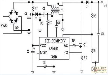
Figure 4 FAN6961 peripheral circuit
From the following equation, we find that the current stress of the switch S is: 1.93A.

Formula 1
Since the PFC stage output voltage range is 400 ± 20V, V0_max = 420V, consider selecting the PDPF20N50 switching transistor (VDS=500V, ID=12.9A, RDS(on)=0.2Ω).
In order to reduce noise, the switching frequency of the Boost converter should be as low as possible, but it must be greater than 20 kHz (below the 20 kHz human ear can hear). In this study, fmin=40 kHz is set. At this time, the effective value of the input voltage is VRMS=265V, Vin=√2VRMS=374V, V0=400V, and the input power Pin=P0/η=150/0.85=176.5W. Substituting the following formula: L = 220H.