In order to provide more functionality, the chip has become larger and larger, but on the contrary, the package has been required to accommodate these larger sized chips in smaller sizes. This inevitably requires that new candidate packaging technologies can both increase system efficiency and reduce manufacturing costs.
Areas covered by package innovation include a wider range of current ratings and voltage ratings, thermal and fault protection mechanisms. This article lists the key factors engineers need to consider when evaluating package technology characteristics for semiconductor devices.
We start with the most common doubts: small package sizes.
1. Smaller package size
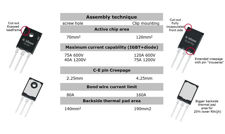
Now, we hope that IC packaging can save board space, help achieve a more robust design, and reduce PCB assembly costs by eliminating some external components. As a result, the industry is optimizing IC packaging technologies such as D2PAK 7 to increase die size by up to 20% in the same size and lead-out area.
The new package design also offers interchangeable pinout options to maximize size and provide greater design flexibility. This is followed by an in-line or curved plug-in package that helps optimize board space and the required pinout.
The industry is also developing new packages with threshold voltages at logic levels for battery-powered designs that allow microcontrollers to directly drive power devices such as MOSFETs. This also saves board space.
2. Power density
Demand for power chips and modules is growing in products such as motor drives, solar inverters and power supplies, which has driven the need for higher power densities without increasing package size.
How do designers increase power density while maintaining package robustness and reliability? First, the package can use a larger leadframe area to accommodate larger power chips such as IGBTs. This also achieves a lower package thermal resistance, which is beneficial for improving heat dissipation.
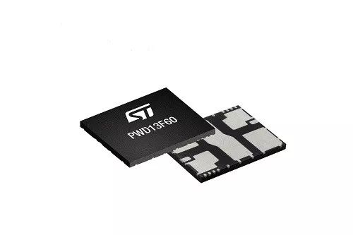
Taking STMicroelectronics' new system-in-package (SiP) PWD13F60 as an example, it integrates four power MOSFETs into a package that is 60% smaller than comparable circuits (Figure 1). The PWD13F60 package integrates a gate driver for the power MOSFET, a bootstrap diode for the upper side drive, cross conduction protection, and undervoltage lockout.

Figure 1: STMicroelectronics' SiP solution for industrial motor drives, lamp ballasts, power supplies, converters and inverter applications.
The shutdown circuit protects the power switch and the undervoltage lockout prevents low voltage faults. Similarly, bootstrap diodes reduce bill of materials (BOM) and simplify board layout.
It demonstrates why package selection is critical to maximizing energy efficiency and adapting to a wide range of supply voltages. Here, it is also worth noting that the power density of the package and the improvement of the heat dissipation conditions are complementary.
3. Heat dissipation efficiency
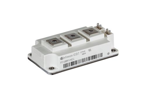
Since devices such as IGBTs operate at lower temperatures to reduce stress on the device, the thermal performance of the package is intrinsically linked to its reliability (Figure 2). Since the size of the heat sink required for lower temperatures is not large, the heat dissipation characteristics also affect the size of the heat sink. In addition, the reduction in cooling requirements also leaves designers with more room to increase power density.

Figure 2: Infineon's power module package uses thermal interface material (TIM).
Some packages retain the package size and high heat dissipation efficiency of the bottom design while the top source is exposed as a heat sink. This allows for higher current ratings for higher power density and smaller package sizes.
4. Cooling
Conventional methods for creating isolation inside the package are often expensive and difficult to handle. Moreover, they are far from enough to manage the heat dissipation of high power density devices such as IGBTs.
As a result, Infineon has introduced a packaging technology called Trenchstop Advanced Isolation (Figure 3). According to the German chipmaker, Trenchtop packaging technology can replace the full isolation package (FullPAK) and standard isolation foil. Infineon positions the new package for applications such as power factor correction (PFC), uninterruptible power supplies (UPS) and power converters for air conditioning.

Figure 3: The heat output of the right package is reduced by 15%.
This isolating package eliminates the need for insulation and thermal grease, allowing designers to reduce assembly time by up to 35%. At the same time, it also improves reliability because there is no misalignment of the separator foil. This also achieves an improvement of 10 ° C lower than the FullPAK operating temperature.
5. Switching loss
Especially for hard switching circuits with operating frequencies up to 20 kHz in devices such as industrial drivers, it is imperative to improve package efficiency and reduce switching losses. In addition, reliable switching and low EMI enhance heat-free operation in low-power applications.
To reduce switching losses, some package solutions use additional Kelvin emitter power pins (Figure 4). It bypasses the emitter lead inductance of the gate control loop, which increases the switching speed of the device and reduces the switching energy.

Figure 4: A package with a Kelvin emitter reduces dynamic losses by 20%.
Ejector Connector,Plug Row Connector,Ejector Header Socket,Ejector Header Connector
Dongguan ZhiChuangXing Electronics Co., LTD , https://www.zcxelectronics.com