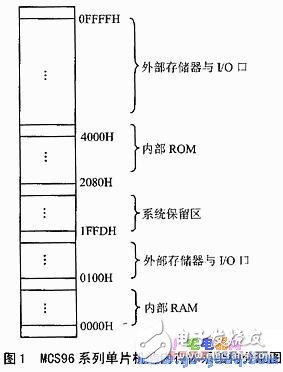
MCS96 series MCU is a kind of 16-bit word length, which is more complete and higher than MCS51 series MCU. It is widely used in instrumentation, process control and other fields. In the application development of MCS96 series MCUs, we have encountered a problem: when large-capacity data storage is required, the expansion of data memory can not work in the same way as the MCS51 series MCU. Because its memory architecture uses the Princeton structure in which the program memory and the data memory are uniformly addressed, the address of the program memory and the address of the data memory cannot be the same; and the MCS51 series MCU uses a Harvard structure in which the program memory and the data memory are separately addressed, and the program memory The address does not conflict with the address of the data memory, can be the same, so its data memory expansion is easy, and the entire data memory address space is continuous. The Princeton memory architecture of the MCS96 family of microcontrollers dictates that the same data memory expansion technology as the MCS51 family of microcontrollers cannot be simply used. This paper presents a segment-managed large-capacity data memory extension technology for the memory architecture features of MCS96 series microcontrollers.
1 segment managed large capacity data storage expansion technologyOverview of design ideas: For the storage structure characteristics of MCS96 series MCU, it can be seen that the lower 16-bit address of the extended data memory cannot be the same as the address of the program memory. Therefore, it is necessary to find a special one from the memory architecture of the MCS96 series MCU. area. In this paper, this area is defined as a segment, which is extended to distinguish different segments by the high address of each segment. Since the actual physical addresses of the segments are disconnected, it is cumbersome to use the physical address programming directly from the user's point of view. Therefore, a logical segment table is designed to be managed, and a simple subroutine is designed to complete the conversion between the logical address and the physical address. To facilitate user programming. The specific process is as follows.
Section 1.1 setting area
According to the memory architecture allocation diagram of the MCS96 series MCU shown in Figure 1, it can be seen that the two areas 0100H to 1FFDH and 4000H to 0FFFFH can be used for external memory and I/O ports. The area of ​​0100H to 1FFDH is small. Considering that the program of the general application system is short, only the same KB and I/O port address are less, so this area can be analyzed to the external program memory and I/O port. The 4000H to 0FFFFH area is allocated to the external data memory. Since the general data storage has a storage address capacity of 2NKB (N is an integer greater than zero), the 48 KB area can be divided into two sections of 32 KB and 16 KB. If a large-capacity storage address space is required, the above 48 KB area can be regarded as a whole segment, or a part of the area can be regarded as a segment, and a plurality of such segments can be set.

The best setting for 1.2 segment storage space
Since the setting area of ​​the space of the segment is in the 48 KB storage address space of 4000H to 0FFFFH, there are three types of storage address space size setting schemes.
1 each segment is set to the same 32KB of the starting address;
2 each section is set to 48KB;
3 Some segments are set to 48KB; some segments are set to 32KB.
Since schemes 2 and 3 use a 32 KB storage interval and a 16 KB storage interval to form a segment, the connection between the address decoder and the memory is complicated in hardware design, and it is inconvenient to manage access to each segment, especially for data storage. When the large-capacity EEPROM or FLASH RAM is used, the hardware design is more difficult; while the scheme 1 only uses 32KB chips, and the starting address is the same. For the data memory, multiple 32KB RAM chips are used, or the data memory is single large. The capacity of the EEPROM or FLASH RAM chip (which can be divided into multiple 32KB segments) is very simple in hardware design, and it is also convenient to use the logical segment table for access management. Therefore, it is necessary to use the scheme 1, that is, the optimal setting of the storage space size of the segment is 32 KB.
White IDC Connector :IDC connector Automotive Connector is a kind of component that electronic engineering and technical personnel often contact. Its function is very simple: in the circuit is blocked or isolated between the circuit, set up a bridge of communication, so that the current flow, so that the circuit to achieve the intended function. The form and structure of automobile connector are changeable. It is mainly composed of four basic structural components: contact, shell (depending on the variety) and insulator.
White IDC Connector
ShenZhen Antenk Electronics Co,Ltd , http://www.coincellholder.com