In recent years, with the further development and improvement of Ethernet technology, especially the improvement of communication rate and the application of interactive technology, it has become possible to apply Ethernet technology in the field of field control, which has a new impact on industrial control networks. From the current trend, Ethernet has entered the field control level, but the existing field bus will continue to exist, and Industrial Ethernet can only occupy a certain market.
In reality, Ethernet expands the existing system, but the field bus cannot be completely replaced by industrial Ethernet. The latter has great potential and its application field will continue to expand. Therefore, it has become a trend to combine fieldbus and Ethernet to achieve tight integration between the underlying production and the upper management. As one of the most widely used fieldbuses in the world, CAN bus has also been widely used in China. The design uses CAN bus as the industrial field bus to realize its interconnection with Ethernet.
1 hardware structure
At present, there are two main methods for designing embedded gateways connected to CAN and Ethernet: one is the design method of low-end MCU plus interface chip, and the other is high-grade MCU plus EOS (real-time multitasking operating system) plus interface chip. Design method. Because CAN only uses the first and second layers of the ISO/OSI reference model, the protocol is relatively simple, and it is suitable for discrete control systems with low cost and low rate requirements. Considering the reasonable cost and the effective utilization of processing power, the design adopts the method of low-end MCU plus interface chip, and its hardware block diagram is shown in Figure 1.
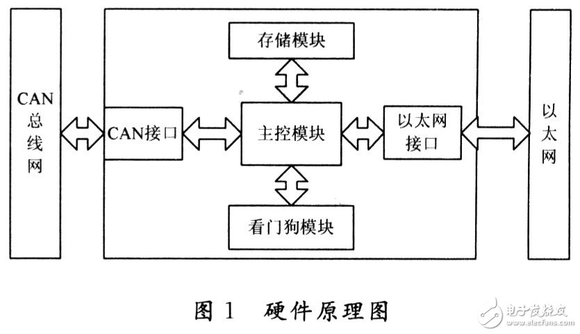
1.1 main control chip and Ethernet interface module
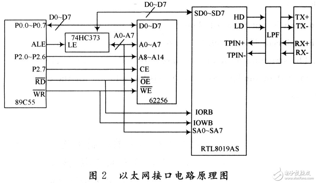
According to the requirements, the system selected AT89C55 single-chip microcomputer produced by Atmel Company with high performance price. It is oriented to measurement and control objects and embedded applications, so its architecture and CPU, instruction system, peripheral unit circuits are specifically designed according to this requirement. It has up to 20 KB of FLASH program memory, AT89C55 is fully compatible with 8051 instruction set, on-chip FLASH is convenient for users to program online, working at up to 33 MHz, 256 B internal RAM, 32 programmable I/O Port, 3 16-bit timer/counter, 8 interrupt sources, support low-power idle mode. The Ethernet interface uses the RTL8019AS chip, a highly integrated Ethernet controller from Realtek that implements all the functions of the Ethernet Media Access Layer (MAC) and Physical Layer (PHY). There are two RAM areas inside the RTL8019AS: one is 16 KB, the address is 0x4000~0x7fff. To receive and send data packets, you must read and write 16 KB of RAM inside the RTL8019AS through DMA. It is actually dual port RAM, that is, there are two The bus is connected to it, one bus is used for RTL8019AS to read/write or write/read the RAM, ie local DMA; the other bus is used for reading or writing the RAM, ie remote DMA; the second is 32 bytes, the address is 0x0000~ 0x001F, used to store the Ethernet physical address. The hardware interface schematic diagram of the main control chip and Ethernet interface chip is shown in Figure 2. It is worth noting that since the Ethernet packet can exceed 1 500 bytes at most, the AT89C55's on-chip RAM has only 256 bytes, so it is impossible to store such a large packet, so a 32 KB external RAM is extended here. Can also improve the data transmission speed of the microcontroller.
1.2 CAN interface module
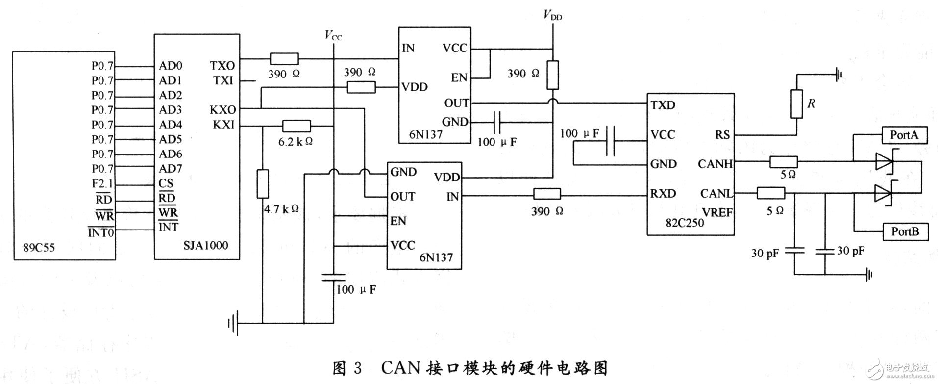
The main components that make up the CAN system are the CAN controller and transceiver. In this design, the CAN interface module uses the SJA1000 chip and the PCA82C250 chip. The SJA1000 is a stand-alone CAN controller that is a replacement for another PC controller, the PCA82C200 from Philips, and adds a new operating mode (Peli CAN) that supports the CAN 2.0B protocol. SJA1000 mainly completes the CAN communication protocol, which realizes the assembly and splitting of messages, filtering and verification of received information.
The PCA82C250 is the interface between the CAN controller and the physical bus and is used to enhance the drive capability of the system. In a transceiver-based system, the number of nodes can be at least 110, while also reducing radio frequency interference (RFI) and strong immunity to electromagnetic interference (EMI). There are several places to pay special attention to when dealing with this part of the circuit:
(1) Problems with the crystal oscillator circuit. Both the 89C55 and the SJA1000 should have separate crystal oscillator circuits. It is not possible to drive the microcontroller with the clock output signal CLKOUT of the SJA1000.
(2) The problem of the reset pin. Although the reset of the SJA1000 is low, it cannot be directly connected to the reset pin of the microcontroller through a NOT gate. Generally, there are two ways to solve the reset pin problem: the first one is to use the I/O pin of the microcontroller to control the reset pin of SJA. The advantage is that the MCU can completely control the reset process of SJA; the second is to adopt appropriate To reset the chip, the design is the first method to reduce costs.
(3) The potential of the RX1 pin must be maintained at approximately 0.5 VCC, otherwise the logic level required by the CAN protocol will not be formed.
(4) It is necessary to pay attention to the terminal impedance matching of the cable, which directly affects whether the CAN bus can work normally and network performance. The hardware circuit diagram of the CAN interface module is shown in Figure 3. A slope resistor R is connected to the RS pin of the PCA82C250, and the size of the resistor can be appropriately adjusted according to the bus communication speed.
2 communication module software design
2.1 SJA1000 driver implementation
The SJA1000 driver is composed of the SJA initialization function, the send function, and the receive function. Figure 4 shows its flowchart.
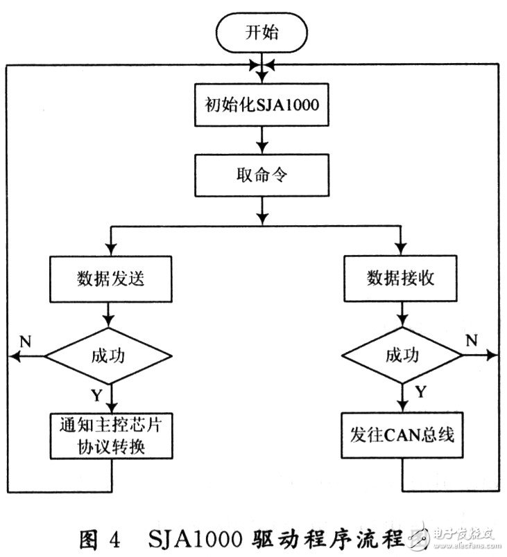
(1) Initialization of SJA1000. The SJA1000 needs to be initialized after the system is powered on, hardware reset or the host controller issues a reset command to set important parameters such as its operating mode, communication rate, output control mode and identifier mask format. The initialization of the CAN controller SJA1000 can only be done in reset mode. The flow chart of the program is shown in Figure 4.
First, the program detects whether the CAN interface works normally, that is, writes and reads to the test register of SJA1000, and verifies whether the results are consistent. If the result is consistent, it enters the reset mode for initial setting. During the initialization process, if the setting of a certain register has not been completed for more than the specified time, the initialization is considered to be invalid, and the initialization program automatically sends an error signal.
(2) Transmission and reception of data. The SJA1000 chip has a message transmission buffer and two message reception buffers for CAN message transmission. The data is sent from the CAN controller SJA1000 to the CAN bus, which is automatically completed by the CAN controller. The data transmission program extracts the data to be sent in the data storage area, forms an information frame, and fills the frame ID of the host with the frame header; Send the information frame to the send buffer of the CAN controller; finally start the send command. Information from the CAN bus to the CAN receive buffer is also done automatically by the CAN controller. The receiving program only needs to read the information to be received from the receiving buffer and store it in the data storage area.
2.2 Implementation of RTL8019AS Driver
The driver of RTL8019AS is the same as the driver of SJA. It has three functions: chip initialization, receiving and sending.
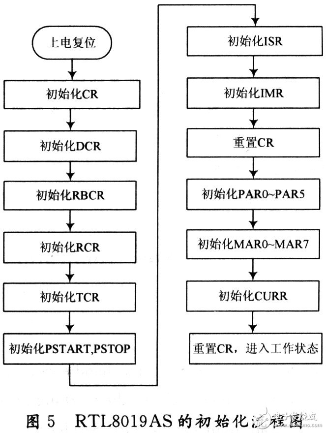
(1) Initialization of RTL8019AS. The initialization process of RTL8019AS is more complicated, but it is very important, it determines some important parameters in the communication process. For example, set the register of the relevant working mode, allocate and initialize the receiving and sending buffers, initialize the network card receiving address, etc., and the flow chart is shown in Figure 5.
(2) Transmission and reception of data. Because the physical address setting of the Ethernet has been completed in the initialization routine of the RTL8019AS, and the transmit buffer start page address register TPSR is specified. In addition, the RTL8019AS CRC check auto generator is also enabled, so the RTL8019AS packet sending procedure is relatively simple. During the transmission of the data packet, the AT89C55 only needs to write the data packet to be sent to the transmission buffer of the RTL8019AS on-chip SRAM through remote DMA, and start the transmission process.
When receiving data packets, there are two ways of query and interrupt. In view of the limited processing capability of AT89C55, the query mode is adopted in the design. According to the judgment CURB==BNRY+1, it can be judged whether new packets are received, if any The data is then read from the network card chip RAM by a DMA read operation.
2.3 Gateway Protocol Conversion Process
The embedded network interface enables interconnection of two networks. When the Ethernet application layer has data to send to the CAN node, the data is first sent to the gateway, and the complete CAN protocol packet is parsed by the Ethernet controller protocol conversion module and sent to the CAN bus through the CAN controller. Conversely, when the CAN device has data to send to the user layer, the data is first sent to the transparent gateway, and the complete CAN protocol data packet is stored in the buffer by the CAN controller protocol module, and then the main control chip is notified, and the Ethernet is called by it. The network control protocol conversion module encapsulates the complete CAN protocol data packet as application layer data and then sends it to the application layer of the Ethernet.
3 Conclusion
Introduced here is a low-cost, high-reliability, fast CAN Ethernet gateway hardware and software design. Through practical application, the design can be used as a module of the CAN bus node, which can be combined with instruments and other equipment. To make it have the ability of network communication, compare the design of similar products, the design can greatly improve its cost performance
Which is the most welcome kid laptop for entertainment and online learning? 10.1 inch laptop is the best choice. You can see netbook 10.1 inch with android os, 10.1 inch windows laptop, mini laptop 10.1 inch 2 in 1 windows, 10.1 inch 2 In 1 Laptop with android os. Of course, there are various matches of memory and storage, 2 32GB or 4 64GB. Our suggestion is that 10.1 inch android 32GB laptop, 10.1inch 32GB or 64GB Solid State Drive windows laptop. Except 10.1 inch Student Laptop , there are 11 Inch Laptop, 15.6 Inch Laptop, 14 Inch Laptop , also option here.
Besides, other advantages you can see on 10.1inch Budget Laptop For Students, for example, lightweight, competitive cost, portability, Android or Windows OS, rich slots, energy saving cpu, etc.
As a professional manufacturer, can provide free custom service, like mark client`s logo on laptop cover, opening system, inner color box, manual, boot. Produce as your special requirement on parameters, preinstall apps needed, etc. What you need to do is very simple, confirming PI, including price, delivery time, parameters, etc.
10.1 Inch Laptop,Netbook 10.1 Inch,10.1 Inch 2 In 1 Laptop,10.1 Inch Windows Laptop,Mini Laptop 10.1 Inch
Henan Shuyi Electronics Co., Ltd. , https://www.shuyihost.com